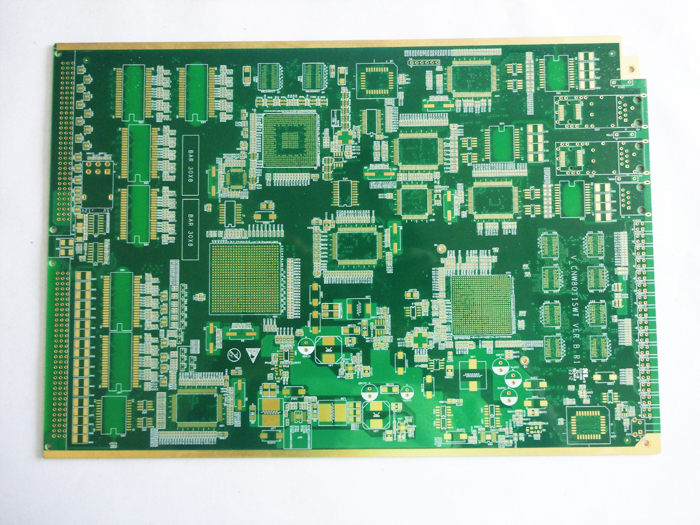
Generally, the requirements for the structure design and process manufacturing of multi-layer circuit boards are very high, and the higher the number of layers, the more difficult it is. Suitable for use in more complex circuits. So what are the advantages of using multilayer circuit boards, let’s learn together
1. The advantages of using multi-layer boards are: high assembly density and small size; the connection between electronic components is shortened, and the signal transmission speed is improved; it is convenient for wiring; for high-frequency circuits, a ground layer is added to make the signal line to the ground A constant low impedance is formed; the shielding effect is good. However, the more layers, the higher the cost, the longer the processing cycle, and the more troublesome quality inspection.
2. In addition, from the perspective of cost, when comparing the cost of the same area, although the cost of a multi-layer circuit board is higher than that of a single-layer circuit board, if other factors such as the miniaturization of the circuit board and the convenience of reducing noise are taken into consideration, The cost difference between multi-layer circuit boards and single-layer circuit boards is not as high as expected. When simply calculating the area cost of the circuit board according to the data we know, the area of the double-layer circuit board that can be purchased by the daily yuan is about 462mm2, and the area of the 4-layer circuit board is 26mm2, which means that the same circuit is designed, if 4 layers The use area of the circuit board can be reduced to 1/2 of the double-layer board, so the cost is the same as that of the double-layer circuit board. Although multiple layers in batches will affect the cost per unit area of the circuit board, there is still not a 4 times price difference. If a price difference of more than 4 times occurs, as long as you can try to reduce the use area of the circuit board, and try to reduce it to 1% of the double-layer board. /4 or less is fine.
3. Our common computer boards usually use four-layer boards or six-layer boards, but now there are more than 100 layers of practical printed circuit boards. The difference between a six-layer board and a four-layer board is in the middle, that is, there are two more internal signal layers between the ground layer and the power layer, which are thicker than the four-layer board.

4. Multilayer boards are actually made by laminating and bonding several etched single or double panels. The double panel is easy to distinguish. Looking at the light, except for the wiring on both sides, other places are transparent. For the four-layer board and the six-layer board, because the layers in the circuit board are very tightly combined, if there are corresponding marks on the board, there is no good way to distinguish.
5. For simple circuits such as radios, single-sided or double-sided manufacturing is sufficient. However, with the development of microelectronics technology, the complexity of circuits has greatly increased, and higher requirements have been placed on the electrical performance of circuit boards. If single-sided or double-sided boards are used, the circuit volume will be very large, and the wiring will also be used. It is very difficult. In addition, the electromagnetic interference between the lines is not easy to handle, so a multi-layer board appears (the number of layers means there are several independent wiring layers, usually an even number).
6, PCB circuit board manufacturers have three or more layers of conductor patterns for multilayer printed circuit boards, and the conductor layers are divided into inner and outer layers. The inner layer is a conductor pattern completely sandwiched inside the multilayer board; the outer layer is a conductor pattern on the surface of the multilayer board. Generally, the inner conductor pattern is processed first during production, and the hole and the outer conductor pattern are processed after pressing, and the inner and outer layers are connected by metalized holes.