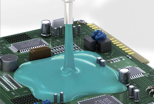
PCB process, solder bead probe technology, increase ICT test coverage
Solder bead probe technology in the processing of PCBA electronic products uses existing wiring to increase the test point coverage of In-Circuit-Test without the need for additional circuit board space, that is, increase the test points on the printed circuit board (Test Point), in order to achieve the purpose of using ICT to test the assembled circuit board.
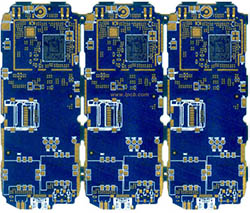
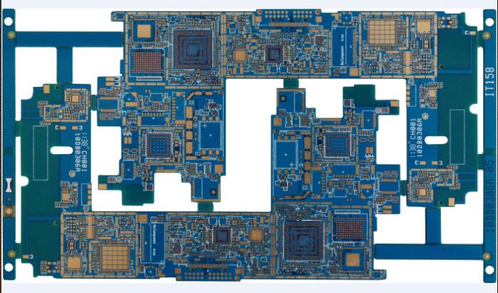
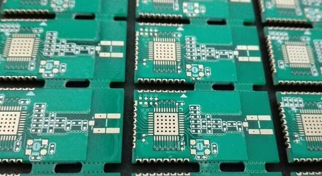
Because the density of the parts on the circuit board is getting denser, but the space is getting smaller and smaller, especially for the board of a mobile phone, so the first thing that is sacrificed is the test point without any function, because many bosses think: quality It is manufactured, so as long as the quality of the circuit board assembly is good, there is no need for subsequent electrical testing. I totally agree with this sentence. It’s just that at the current pace of rapid advancement in the electronics industry, a case will be completed in nine or even six months. I really don’t know that there is an engineer who can pack a ticket and say that the product he designed has no bugs and is assembled. The factory dare not say that they can assemble zero defects with zero boards? Up to now, BGA packages have been big enough for SMT and process engineers. Now a bunch of new IC packages (such as QFN) have appeared, and the entire communication module is built on a small circuit board. The finished product factory needs to put this The whole module circuit board is regarded as an SMT part and is soldered on the circuit board.

Various design and electronic circuit assembly challenges are now showing that it is difficult to abandon traditional ICT, and only use other methods (such as AOI, AXI) to ensure the quality of PCB Assembly, so there are more More and more companies have come back to use ICT, but the space on the circuit board will only get smaller and smaller. There is no room for testing points, so I came up with this kind of solder paste printing on the existing wiring. Way to replace the bead probe technology (bead probe) method of test points, the purpose of course is to hope that the entire electronics industry can continue to maintain ICT operations, and then purchase more of its 3070 series ICT test machines.
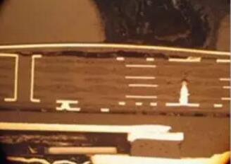
The traditional ICT test method uses a pointed probe to contact a circular test point to form a loop. This method requires a large area of test point, and then the probe must be shot to the target just like an archery. In the range of the target, it needs to use a lot of circuit board space; while the bead probe technology is just upside down, it hopes that the test point should not occupy the space of the circuit board as much as possible, but in order to contact the probe to form a loop, So printed solder paste to make the test point higher, and then use a larger diameter flat-head probe (50, 75, 100 mils) to increase the chance of contact with the test point, just like knocking an iron nail with a hammer.
In theory, this is really a breakthrough in the rebirth of test points, but there are still many technologies that need to be overcome in the real environment:
The solder paste printed on the wiring is likely to affect the problem of poor contact between the probe and the test point due to the residual flux. In response to this problem, a number of probe manufacturers have designed probes for use with bead probe technology.
The printing of solder paste must be very precise. In particular, the cohesion of lead-free solder paste is worse than that of tin-lead solder paste, and more precise solder paste printing is required, because the high tin print volume will determine the height of the solder. If the solder height on the test point is not enough, ICT misjudgment The rate will increase. This involves the printing process of the solder paste, the precision of the steel plate, and the tolerances when the circuit board is assembled.
If the width of the PCB wiring is too small, it is easy to be inadvertently inferred by probes or other external forces due to insufficient adhesion. It is generally recommended that the minimum wiring width should be more than 5mils. It is said that the industry has successfully tested 4mils, but as the width of the wiring is smaller, the false positive rate of its ICT is higher. It is recommended to increase the width of the wiring and cover it with green paint (mask) to make it stronger.