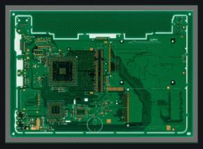
In today's developed industry, PCB circuit boards are widely used in various lines of electronic products. According to different industries, the color and shape, size, level, and materials of PCB circuit boards are different. Therefore, clear information is needed in the design of the PCB board, otherwise misunderstandings are prone to appear. This article summarizes the ten major defects based on the PCB design process.
1. The processing level is not clearly defined
The single-sided board is designed on the TOP layer. If the front and back are not specified, it may be difficult to solder the board with components.
2. The large area of copper foil is too close to the outer frame
The distance between the large area copper foil and the outer frame should be at least 0.2mm, because when milling the shape of the copper foil, it is easy to cause the copper foil to warp and cause the solder resist to fall off.
3. Draw pads with filling blocks
Drawing pads with filler blocks can pass the DRC inspection when designing the circuit, but it is not good for processing. Therefore, similar pads cannot directly generate solder mask data. When the solder resist is applied, the filler block area will be covered by the solder resist, resulting in the device Difficulty in welding.
Fourth, the electrical ground layer is also a flower pad and a connection

Because it is designed as a flower pad power supply, the ground layer is opposite to the actual printed board image. All connections are isolated lines. When drawing several sets of power or ground isolation lines, you should be careful not to leave gaps so that the two sets A short-circuit of the power supply cannot cause the connection area to be blocked.
Five, random characters
The SMD soldering pad of the character cover pad brings inconvenience to the continuity test of the printed board and the soldering of the components. The character design is too small, making screen printing difficult, and too large will cause the characters to overlap each other and make it difficult to distinguish.
Sixth, the surface mount device pad is too short
This is for the continuity test. For too dense surface mount devices, the spacing between the two pins is quite small, and the pads are also quite thin. The test pins must be installed in staggered positions. If the pad design is too short, although it is not Affect the device installation, but will make the test pin staggered.
Seven, single-sided pad aperture setting
Single-sided pads are generally not drilled. If the drilled holes need to be marked, the hole diameter should be designed to be zero. If the value is designed, then when the drilling data is generated, the hole coordinates will appear at this position, and there will be a problem. Single-sided pads such as drilling should be specially marked.
Eight, the pad overlap
In the drilling process, the drill bit will be broken due to multiple drilling in one place, resulting in hole damage. The two holes in the multi-layer board overlapped, and the negative film appeared as an isolation disk after drawing, resulting in scrap.
Nine, there are too many filling blocks in the design or the filling blocks are filled with very thin lines
The gerber data is lost, and the gerber data is incomplete. Because the filling block is drawn with lines one by one during the light drawing data processing, the amount of light drawing data generated is quite large, which increases the difficulty of data processing.
X. Graphic layer abuse
Some useless connections were made on some graphics layers, but the original four-layer board was designed with more than five layers, which caused misunderstandings. Violation of conventional design. The graphic layer should be kept intact and clear when designing.
The above is a summary of the ten major defects in the PCB board design process. According to us, we can improve the production schedule of the PCB board and reduce the occurrence of errors as much as possible.