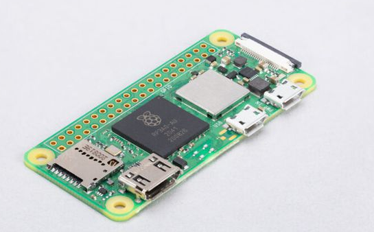
According to relevant definitions, Build up Multilayer PCB (BUM) refers to the formation of an insulating substrate, or a traditional double-sided or multi-layer board, which is formed by coating an insulating medium and then electroless copper plating and copper electroplating. The wires and connecting holes are superimposed so many times to accumulate to form the required number of layers of multi-layer printed boards. As early as the 1970s, there have been reports of BUM technology in the literature, but it was not until the early 1990s that photosensitive resin was coated on the core board, the photo-induced method was used to form the via interconnection, and the additive method was a new process for circuit manufacturing. After the new method of high-density circuit board, this kind of high-density circuit board was successfully used in Thinkpad notebook computers. The new technology was first published in 1991, called Surface Laminar Circuit, SLC (Surface Laminar Circuit, SLC). PCB), because this technology has created an unprecedented High Density Interconnect, HDI (High Density Interconnect) new ideas, unveiled the BM in the history of PCB development abroad. BUM adapts to the requirements of electronic products to be lighter, smaller, thinner and shorter, and can meet the needs of new generation electronic packaging technologies (such as BGA, CSP, MCM, FCP, etc.), so it has developed very rapidly throughout the 1990s, Mainly used in portable electronic products, such as laptop computers, mobile phones, digital cameras and MCM packaging substrates. The world BUM microplate market was 1.1 billion U.S. dollars in 1998, and it reached nearly 2 billion U.S. dollars in 1999. 90% of the market is concentrated in foreign countries, and the 2000 market may be close to 3 billion U.S. dollars. Domestic experts once predicted that the world BUM board has entered a development period; at present and in the next few years, the technological change and market competition in the PCB industry will revolve around the BUM board as the center and its surrounding industries (materials, equipment and testing, etc.) .

1. Introduction to the manufacturing process of the build-up method multi-layer board
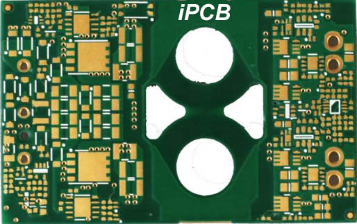
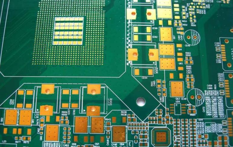
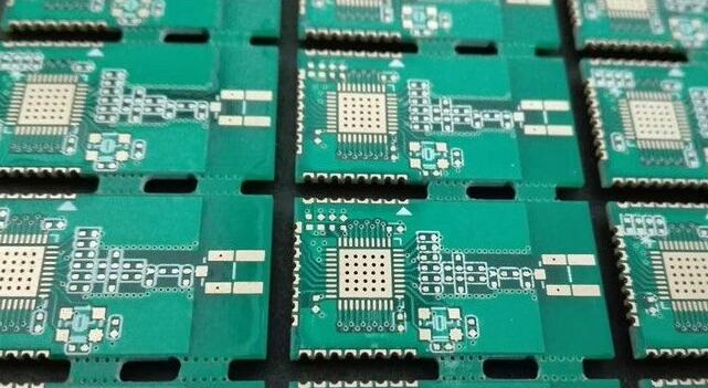
BUM (multilayer circuit board) corresponds to HDI (high density interconnect). In fact, these two terms express almost the same conceptual connotation. According to IPC data, the definition of HDI includes the following: non-mechanical drilling diameter is less than 0.15mm (6mil), and most of them are blind holes (buried holes), and the ring diameter of annular ring, pad or land is less than 0.25mm (6mil), the holes that meet this condition are called micmovia; PCBs with microvias have a contact density of 130 points/inch2 or more, and the wiring density (set the channel width as 50mil) at 117 inches/inch2 The above is called HDI PCB, and its line width/line spacing (L/S) is 3mil /3mil or less. It can be seen that the most essential feature of build-up multilayer circuit boards is high-density interconnection (HDI).
Second, the manufacturing process of multi-layer multi-layer boards
The main difference between BUM and the traditional PCB manufacturing process lies in the hole forming method. The key technologies of BUM mainly include the dielectric material used in the laminated insulating layer; the hole forming technology of microvia; and the hole metallization technology.
Layered insulating dielectric material
Due to the difference between the insulating layer material and the interconnection micro-hole processing method, dozens of different BUM manufacturing methods have appeared, but according to the difference of the laminated insulating dielectric materials used in various BUM manufacturing processes, it is representative and application comparison Mature processes can be divided into three types: resin coated copper foil (RCC) process, thermosetting resin (dry film or liquid) process, and photosensitive resin (dry film or liquid) process. These three processes are now in use. The latter two processes generally need to achieve metallization and circuitization through an additive process, which has high requirements for materials and corresponding technologies. The RCC process adopts the subtractive process to complete the wiring, does not require a large investment in equipment (the main investment is laser driller), and adapts to the traditional multilayer PCB manufacturing process, and the finished BUM board has good performance and reliability, so There are more and more manufacturers using RCC technology to make BUM boards, and the demand for RCC continues to increase. Taking the RCC process as an example, the more the number of buildups, the worse the flatness of the board surface. Due to this limitation, the buildup layer of BUM on the core board generally does not exceed 4 layers.