The goal of PCB design is to create a fully functional circuit board, which I totally agree with. However, my first goal during PCB layout is to make the circuit board 100% routed. The layout must first set the design parameters, and then place the components to meet its electrical, mechanical, and manufacturing requirements. The only thing left after that is to connect all the networks together. It should sound easy, right? Sometimes this is the case, but most of the time it is more complicated than people realize.
To successfully route printed circuit boards, many details must be considered and resolved. For example, power and ground wires must be configured to provide a good clean signal return path for sensitive networks, and traces carrying sensitive signals must have a certain width and be far away from high-noise circuits that may affect its operation. These are just some of the things that designers need to consider when wiring the circuit board. In the third part of a four-part series of circuit board design, here are some of the best practices for PCB routing in more detail.

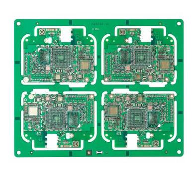
Good PCB wiring habits start with the pcb layout best practices of any traces
In the first part of this series, the best PCB design practices for developing schematics for printed circuit board design are studied. Using the schematic as the basis for the design, I saw some layout best practices for placing components on the design in the second part of the series. Now, in the third part, you will see how all the preparations that have been done so far will help place the network connections between these placed components.
However, before completing the wiring, it is best to check the design and make sure you are ready for the next step:
Has the database been properly configured with the approved layer stack?
Have all design rules and any unique wiring constraints been installed?
Are all the components on the board?
Is the component placement optimized for the best connection mode?
Assuming all these items have been completed, you can start tracking route.
Nine pcb layout best practices for circuit board design
There are many different types and styles of traces that need to be routed on the circuit board, and these nine best practices will cover most of the methods you will use:
Routing tools: The first step in routing a circuit board is to make sure you understand how to use the design tools you are using. It is not uncommon to find that designers waste time on manual wiring tasks, because they do not know that the automation features in the tool will do better.
Escape routing: All pins of high-pin count components (such as 600-pin BGA processor chips) must be routed to vias so that they can be connected to the inner layer. In-pad vias and microvias are usually used for escape wiring, and bypass caps and other small discrete parts connected to these same pins are usually wired at the same time.
Power supply: Use short and wide traces to route power circuits to help reduce trace inductance and control electromagnetic interference (EMI) and heat. When routing these traces or rounded corners, it is best to use a 45-degree angle. It is best to keep the wiring on one layer and avoid the use of vias, because vias require optimal placement of power components.
Signal path: In high-speed circuits, the signal path is very important. It is important to use short direct traces to connect these networks. Like the power supply, this largely depends on the placement of the parts, and the schematic should be used as a guide for placement and wiring.
High-speed transmission lines: Due to the need to control the energy of the transmission lines, these traces should be routed on the inner layer immediately adjacent to the two reference plane layers or between the two reference plane layers. This is called a microstrip or stripline layer configuration and is essential to provide the clearest and most direct signal return path. This is also important when routing transmission lines without crossing separate planes, as this may disrupt the signal return path, thereby generating a lot of unnecessary noise on the board. There are many forms of high-speed transmission lines. Your PCB design CAD tools usually have some built-in functions for routing controlled impedance lines, differential pairs or sensitive signals that require additional spacing.
Bus routing: Digital circuits will usually have a network group to be routed, called a bus. These buses are usually data and address lines between the processor and memory components, so high-speed design constraints may be added. The buses should be routed together so that their length matches the signal timing, and some CAD systems provide specialized automatic interactive routing functions for these networks together.
Analog routing: Analog routing should be isolated from digital routing as much as possible. It should have its own separate reference plane for signal return to prevent analog signal noise from polluting the digital circuit.
Power and ground wires: The power and ground wires should be wide, especially for circuits with higher currents. Remember to use a heat sink for the connection of through-hole pins and discrete components to prevent thermal imbalance during soldering. When possible, it is best to use a solid metal plane, and the ground plane should be far away from slots, cuts and cracks to serve as a clear signal return path. If it is unavoidable to use a split plane, make sure that the split is not in the area of high-speed wiring.
Cleanup: This is more than just making the routing look neat. In some cases, such as floating traces, it may affect the signal integrity of the circuit board because they behave as if the antenna is radiating energy. Make sure to use the tools you need to find and correct any problems remaining in the routing.
These nine pcb layout best practices can complete most of the trace routing required in PCB design.