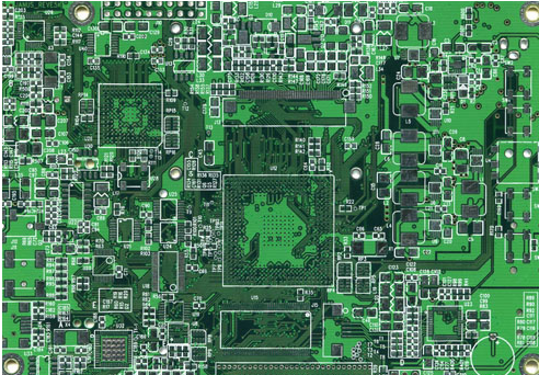
In PCB circuit board design, unlike the traditional method of dividing the design into several parts and completing each part independently, this new technology can create parallel processes on a common database, and can automatically synchronize process changes and solve possible mutual problems. conflict. This is the first in the EDA industry.
Since the widespread adoption of CAD in circuit board design in the 1990s, the manufacturing field has been continuously improving design productivity through automation and process optimization methods. Unfortunately, with the continuous innovation of circuit design software technology, the demand for supporting new signals, components or board-level manufacturing technologies is also increasing, so the entire design time has hardly been shortened (or even longer).
If there is no fundamental change in design methodology, software will always play the role of a follower of hardware technology, rather than becoming a leader on the development curve. The concurrent engineering technology of multiple engineers working on the same design has always been an effective magic weapon for productivity breakthroughs. The traditional divide-and-conquer method divides the design into several parts and assigns them to the hands of each engineer, and finally connects the various parts, and uses coercive measures (automatically make decisions according to predefined rules) or clever means (allow engineers to resolve conflicts one by one) ) Resolve all conflicts.
This method is quite effective for circuit schematic design, because it can directly divide the design into multiple modules and pages according to functions. Even so, this method still requires a lot of manual operations to solve the interconnection problems between modules, such as signal name conflicts, missing components, and so on. As long as the designers can't see what each other is doing, these mistakes are very likely to happen.
If a parallel design method allows multiple designers to do the same design at the same time, can see the editing content made by other designers, and can automatically manage various potential conflicts in real time, then this parallel design method can be achieved. Optimal flexibility and productivity.
1. Parallel design architecture
The new concurrent design technology requires a design process manager (server) and multiple design clients running in a network environment. The main job of the server software is to receive update requests from each client, check the requests to ensure that no design rules are violated, and then synchronize each client according to the update content.
Each client must have its own dedicated processor and memory. The new parallel design architecture also assumes that the communication system can support the minimum bandwidth and maximum delay required for real-time and efficient exchange of information between the client and the server. Each client can see the entire design and observe other client edits as the server processes them. The design database is allowed to be stored anywhere on the network.
This parallel design architecture allows multiple designers to do the same design at the same time without having to divide the design logically or in any other way. This is a truly real-time collaborative design environment, in which all issues related to segmentation boundaries and managing data integrity during segmentation-join operations will not arise.

Since multiple designers can do the same design in parallel without any restrictions, the entire design cycle can be significantly shortened.
Each design has a related design team, and only members of the team are allowed to access the design data. Any team member can start a design meeting on the server and a single client. Other clients can participate in the conference at any time.
The design is initially loaded on the server. When the client joins the meeting and automatically downloads the current state of the server design to the client's memory, the client is initialized and synchronized. Once the client joins the design meeting, it can edit the design using standard editing tools available in the application.
The edit event is an independent activity initiated by the client, and it is sent to the server as an update request. For example, moving a device from point A to point B constitutes an editing event. The beginning of the event is to select the device, and the end of the event is to indicate the new position with a mouse click (or equivalent input). The edit event is sent to the server as a transaction, which describes what to delete and what to add.
Each edit event generated by the client must perform a local design rule check (DRC) before being sent to the server, and then set the priority of the edit request and enter the input message queue according to the first-in first-out principle. After the server receives the editing request, it integrates it into the design database, and then executes DRC. If no problems are found, the edit request is approved and sent to all clients through the output message queue for synchronization of the client's internal core database.
Most of the computing time is spent on the local client. Target objects are added, edited, and deleted on the client side, and all automated operations related to those edits (such as pushing, squeezing, and smoothing) are performed at the same time. Compared with the client, the load of the server is relatively lighter, so the system performance will not be affected. Testing of this environment shows that the server's response speed is very fast and will not slow down the client's speed.
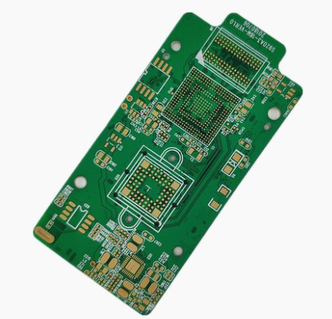
2. Automatic wiring of circuit boards
The second application of concurrent design technology is the automatic wiring of circuit boards. Distributed automatic wiring has been a "powerful weapon" of circuit board wiring software for many years. Previously, IC routers have been converted to run in a distributed environment. However, the circuit board wiring problem is very different. Until now, people still think that the automatic router must be adapted to make full use of the advantages of multiple computers to complete the same design. Software vendors and third-party engineers have also made many attempts to achieve acceptable performance improvements, but they all ended in failure.
The architecture adopted by the new parallel design technology can solve most of the key problems in the distributed wiring environment, and it knows how to prevent or resolve conflicts. Similarly, the server plays the role of design process management, and requests from each auto-router client are integrated, checked, and broadcast to other clients in the server. All auto-router clients are kept in sync, so when a new wiring path is added locally, the probability of wiring path conflicts is small.
3. Integrate efficient tools
Since circuit design is a process that includes many steps and rules, in order to obtain excellent productivity, the most efficient point tools must be closely integrated. Data and rules must flow smoothly throughout the design process.
In the past 20 years, the EDA industry has undergone unprecedented mergers and acquisitions. As a result, the design process of software vendors relies on the integration of many tools. In addition, large companies require the tools of many software vendors to be integrated into their own unique design process.
The stopgap measure is to write an interface through which the ASCII output of one tool is converted into the ASCII input format of other tools. In doing so, hundreds of ASCII interfaces will be generated, and each interface is used to overcome common data model and rule incompatibility issues.
The basic requirement of this integration method is that all applications must have fully compatible data models. Each application may use different tools and different levels of automation when processing data, but each application must be able to receive changes and recognize them so that they know what to do next.
It is also possible to use parallel design techniques to integrate an application to perform a specific set of tasks, such as creating, placing, routing, and editing embedded devices. If so, then that application can be automatically restricted to only allow the use of those specific functions.
4. Circuit and board design
Combining the parallel layout and the technologies required for parallel integration can form an environment where multiple different applications in the design process can be integrated and used by multiple designers at the same time.
For example, the parallel design method of circuit board design, schematic design, constraint management, layout design, three-dimensional mechanical design simulation and manufacturing applications can be integrated in some way, allowing all these applications to be put into use simultaneously, and at the same time Update and synchronize all editing events throughout the design process. Even in a mixed environment, multiple similar applications may appear, such as multiple layout tools.
Since multiple applications are running at the same time, engineers can quickly understand the signal integrity effects of the added path. For example, in a three-dimensional mechanical system designed for a cellular phone, the movement of the device in the layout can be updated and checked immediately.