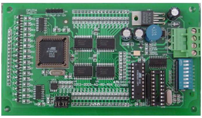
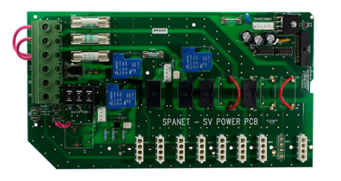
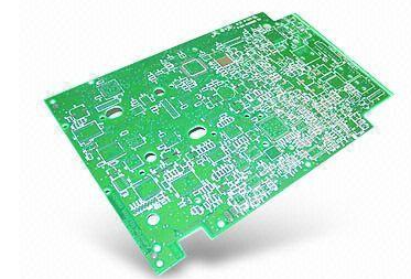
Simply put, the so-called automatic X-ray inspection or AXI technology uses X-rays to check the characteristics of the target object. As an application, it occupies a place in many industries today, including but not limited to aerospace, medical, PCB assembly, etc.
X-rays, as traditional inspection equipment, have a long way to go in testing the quality of PCBs, especially when miniaturization is increasing, they have their own limitations. In addition, there are hidden solder joints in some cases. However, X-rays can also penetrate and check the quality of hidden solder joints. Therefore, although automatic optical inspection is only suitable for relatively easy-to-find defects, such as open circuits or solder bridges, if the light cannot be inspected alone, an automatic X-ray inspection is required.
What are the reasons for choosing automatic X-ray inspection technology in PCB assembly
The advantage of X-rays is that materials absorb X-rays proportional to their atomic weight and depend on their density and thickness. Compared to lighter elements, heavier elements therefore absorb more X-rays. Therefore, hidden defects, such as lack of electrical components, short circuits, etc., are easily captured.

The ideal X-ray system must have clear images so that the information about defect analysis is clear and feasible. Therefore, it is ideal that the X-ray inspection system has sufficient magnification and tilt angle inspection functions. The latter ensures that the solder balls are not only inspected from above.
X-ray inspection equipment usually comes in two forms-two-dimensional and three-dimensional systems. Both of these can be operated offline, thus making the inspection process easy. However, some devices can be used online. The choice of offline and online equipment usually depends on the amount of inspection required. When a large number of inspections are required and the inspection level is complicated, online equipment is usually used. Although the two-dimensional system can display 2D images from components on both sides, the three-dimensional system can generate cross-sectional images. 3D systems can also combine cross-sectional images through a method called tomography.
The type of resolution required also requires the selection of a suitable X-ray tube. There are usually two types-open and closed. The required magnification also determines the distance between the sample and the X-ray tube. X-ray voltage is another determinant of its penetration ability. With high voltage, objects with high density and thickness can be easily inspected. For a single panel, however, it is sufficient to use low voltage. Similarly, multi-layer boards require high pressure.
Early detection equipment comes with an image intensifier connected to a CCD camera, but the image intensifier has the following limitations:
Limited range-The limited range in turn means that multiple techniques may need to be used to inspect the area. This in turn increases the time for satisfactory inspections. Limited field of view-at a given point in time, an area of 3 to 5 inches in diameter can be inspected. Image blooming-Since the ionizing radiation passing through the edge of the casting is not attenuated, image bleeding may occur at the edge of the image. Increased noise level-The image intensifier produces a noisy image. A clean, noise-free image requires digital processing of the image, which in turn is time consuming and does not keep the process in real time.
However, the above limitations can be alleviated in the following ways. Use direct digital imaging equipment. It not only provides a larger detection area, but also improves the resolution.
Using X-ray inspection, you can do the following:
Perform non-destructive inspections Find short circuits Detect void solder joints Determine component displacement Check semiconductors Check switches, relays, plugs and cable connections
In short, the advantages of automatic X-ray inspection technology are as follows:
Reliable and consistent results shorten inspection time and reduce labor costs. Effective process control, because defects can be found in the early stages of the PCB assembly process, and defects in the remaining PCB components can be prevented.
Therefore, overall, X-ray inspection technology is undoubtedly a boon for PCBA manufacturers, because it can help them significantly improve product quality. Due to the need for high-speed images with sub-micron resolution and extremely high definition, the demand and complexity of X-ray inspection technology will increase. The way forward is to be able to reduce the number of expensive operators, while also eliminating the possibility of human error (if any) during the inspection process. This can be achieved by developing some inspection algorithms to solve these complex problems.