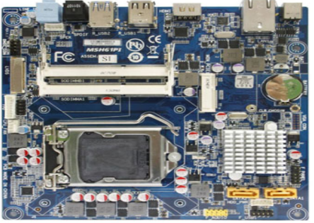
PCB process, double-sided circuit board, multi-layer circuit board quality inspection standard
In fact, many customers are not very clear about the quality inspection standards of double-sided circuit boards and multilayer circuit boards. Today, I will introduce the detailed information of the IPC international inspection standards of circuit boards to everyone, so that everyone can check the quality of PCB correctly.
Scope: This standard applies to the inspection of the product's substrate, metal coating, solder mask, characters, appearance, holes, warpage and other items. When this standard is not suitable for a certain hand-made process or does not meet the requirements of the customer, the standard agreed with the customer shall prevail.
1. Inspection requirements
1 Base (substrate) material:
1.1 White spotted reticulated fibers looming
White spot reticulation is acceptable if it meets the following requirements:
(1) Not more than 5% of the board area
(2) White spots in the line spacing should not occupy 50% of the line spacing
1.2 Halo delamination and blistering are unacceptable.
1.3 Foreign debris
Foreign matter on the substrate is acceptable if it meets the following requirements:
(1) Recognizable as non-conductive substances
(2) The wire spacing is reduced by no more than 50% of the original wire spacing
(3) The longest dimension is not more than 0.75mm
1.4 The base material must not have the copper foil layered and lifted, and there must be no hidden fibers.
1.5 The base material model meets the specified requirements
2 Warpage tolerance (see the table below)
Board thickness tolerance (mm) 0.2-1.2mm or more and 1.5mm or more, double-sided board tolerance ≤1% ≤0.7% multi-layer board tolerance ≤1% ≤0.7%

3 Board thickness tolerance: The thickness of the board meets customer requirements.
The maximum tolerance of the thickness of the rigid product double-sided multilayer board is as follows
Board thickness mm Double panel tolerance mm Multilayer board tolerance mm 0.2-1.0 ±0.1 ±0.1 1.2-1.6 ±0.13 ±0.15 2.0-2.6 ±0.18 ±0.18 Above 3.0 ±0.18±0.2
4 hole requirements:
4.1 The aperture meets customer requirements, and its tolerance range is as follows:
Aperture mm PTH Aperture tolerance mm NPTH Aperture tolerance Less than 1.6mm ±0.08 ±0.05 Greater than 1.6mm ±0.1 ±0.05
Note: The hole position diagram should meet the requirements of the drawing.
4.2 No holes, few holes, undrilled holes, plugged holes, etc. are not allowed.
4.3 There must be no deformed holes (such as round holes drilled into oval holes, horn holes, oval holes drilled into round holes, etc.).
4.4 There should be no copper slag, tin slag, etc. in the hole, which will affect the final hole diameter.
4.5 The copper exposed on the inner wall of the component hole shall not exceed 3 points, and the total area shall not exceed 10% of the hole wall area, and the copper shall not be exposed in a ring shape.
4.6 The cavity area in the hole shall not be greater than 0.5mm, and the number of points for each hole shall not exceed 2, and such holes shall not exceed 5% of the total number of holes. It is not allowed to have ring-shaped cavities in the hole and the corners of the hole to be broken or no copper. All metalized holes connected to the inner layer with electrical appliances on the multilayer board should not have holes.
4.7 Non-conductive via holes are not allowed.
4.8 The coating wrinkles in the hole shall meet the following requirements:
(1) Does not cause poor inner connection.
(2) Meet the requirements of plating thickness.
(3) Good combination with the hole wall.
5 Pad (PAD)
5.1 The pad must be at least 0.1mm, and the ring width of the part connected to the line is reduced by not less than 50% of the line width due to the offset.
5.2 Pinholes and gaps can reduce the area of the pad not to exceed 1/5 of the pad.
5.3 SMD position allows three pinholes within 0.05mm2.
5.4 The pads on the solder resist are as follows (as shown in the icon):
(1) The total area of the pads on any two or three sides shall not exceed 10% of the pads.
(2) The land on a single side shall not exceed 5% of the land area.
Note: The shaded part is solder resist
6 lines
6.1 No short circuit or open circuit is allowed
6.2 Line gaps are allowed, but it should be ensured that the line gaps do not reduce the line width by more than 20% of the design line width. When the line width is greater than 3mm, the line gap or line hole width is less than 1/3 of the line, and the length of the hole or gap If it does not exceed the wire width, it is acceptable, but in this case, there should be no more than two places on the same board.
Note: Notch ---- expose the substrate at the concave point on the edge of the line
6.3 The ratio of the maximum diameter of the pinhole and sand hole to the line width of the line should be less than 1/5, and there should be no more than three places on the same line.
6.4 The conductor width tolerance is not allowed to exceed ±20% of the original design line width. At the same time, it should be ensured that the line spacing tolerance does not exceed ±20% of the original design value.
6.5 The protrusion or depression of a single point of the circuit shall not exceed ±20% of the original design line width.
6.6 The metal residue on each circuit board should not exceed three points, and the line width or line spacing should not increase or decrease by more than 30% of the original design value.
6.7 The line width is not allowed to appear jagged.
6.8 No line distortion is allowed.
7 Solder mask (green oil)
7.1 The type, color and brand of the ink used must be consistent with the ink specified by the customer. If the customer does not specify it, it will be subject to the company's requirements.
7.2 When the customer requests, the color of the solder mask is based on the upper and lower limits of the sample board as the scope of delivery.
7.3 During normal soldering, no blistering of the solder mask or paint peeling off.
7.4 The printing of the solder mask must be uniform on the entire surface and have the same color.
7.5 The repair of solder mask should not exceed three points on the same surface (referring to the board surface above 100mm2), and the length of each location should not be greater than 5mm. The repair should be smooth and uniform in color.
7.6 Stick 3M600# tape tightly on the board surface, and after 30 seconds, pull it up at an angle of 900 to the board surface, and no green oil should fall off.
7.7 The area of the pad on the solder mask of the solder joint of the part foot must not be the arc 900 that intersects the outer ring of the pad.
8.1 The copper foil under the solder mask is not allowed to be oxidized, stained, or scorched.
8.2 Part holes are not allowed to have solder resist into the holes (non-part through holes are required to be sealed according to customer needs).
8.3 In the solder mask, no foreign matter such as lint is allowed to cross two lines, and non-conductive matters such as lint within 1mm in length are allowed to exist, but no more than 2 per square inch.
8.4 The thickness of the solder mask on the line is not less than 10um.
8.5 The waves or lines on the solder mask surface have not yet affected the upper and lower limits of the specified thickness, and slight wrinkles have occurred between the wires, but have not yet caused voids, and the adhesion is good.
8.2 Metal plating and tin spraying layer
9.1 The metal plating layer must not have rough plating or fingerprints.
9.2 The metal coating is tested with 3M600# tape, and there should be no peeling or blistering of the coating.
9.3 The thickness of the coating on the recessed part of the circuit shall not be less than 15 um, and the recessed area shall not exceed 4mm, and no more than two points on each board.
9.4 Plating layer and thickness of spray tin plate
(1) The thickness of the coating should be greater than 3 um, and the thickest should not lead to small holes.
(2) The average thickness of the hole and the plating layer should not be less than 25 um, and the minimum value should not be less than 20 um. The maximum value should not cause the hole to be small.
(3) The tin spraying layer is smooth and bright, and the lead-tin alloy surface has no pollution or discoloration.
9.5 Plating thickness of water gold plate
The minimum thickness of copper plating in the hole is not less than 10 um, the thickness of the nickel plating layer of the circuit is not less than 5 um, and the average thickness of the nickel layer in the hole is not less than 5 um. The gold-plated layer has a uniform golden appearance, with a golden color, no oxidation, pollution and discoloration.
9.6 Metal particles in the circuit part within the formed circuit may be allowed to exist, but the total area shall not be greater than 3mm2, and shall not be greater than 50% of the board edge and the line distance.
9.7 It is not allowed to scratch the exposed substrate by the line. The line scratches on the same side of the unexposed substrate shall not exceed two, and the length shall not exceed 5mm, but the scratch depth shall not exceed 3 um.
9.8 Solder mask scratches should not cause exposure of the metal layer. If the width of the scratch does not exceed 0.05mm and the length does not exceed 5mm, 2 pieces are allowed on the same board.
9.9 There are no more than 3 open-circuit compensation lines for double-sided boards, and they cannot be on the same surface. Only two are allowed for multi-layer boards. The length of the patch line cannot exceed 3mm. The patch line position is 1mm away from the pad, and no patch line is allowed at the corner.
9.10 The wires should not be tinted.
9.11 There should be no obvious milling chips in the shape processing, the edge of the milling processing board should be smooth, the punching shape should be neat, the board edge should be free from bursting defects, and the board surface should not have ink residues, corrosive residues, oil stains, glue stains, finger prints, sweat stains And other pollutants.
10 gold finger
10.1 The thickness of the nickel layer of the gold finger is not less than 5um. When the customer requires the gold finger to be plated with thick gold without specifying the thickness of the plating layer, the gold thickness should not be less than 0.5 um. Less than 0.05 um.
10.3 The golden fingers must not be oxidized, burnt, polluted, or glued, and there must be no residual copper or other foreign matter in the distance, and the color is golden.
10.4 The edge of the golden finger shall not be lifted or damaged.
10.5 The length of the notch on the edge of the golden finger shall not be greater than 0.15mm2, and only one of the golden fingers is allowed to exist on each piece of gold finger. There shall be no more than two such fingers on each board.
10.6 Stick the 3M600# tape on the gold finger, and after 30 seconds, pull it up at a 900 angle to the board surface. There should be no gold or nickel falling off or lifting (that is, gold or nickel).
10.7 Two scratches with a length of 2mm and a depth of less than 3um are allowed in the gold finger, but copper or nickel shall not be exposed. The location of the scratch shall not be 3/5 of the middle part of the gold finger. Such gold fingers are on the same board. No more than two.
10.8 The number of holes, dents, indentations, and cavities of the gold finger are less than 2 points (inclusive), but the length of the gap is within 0.15um, and nickel or copper shall not be exposed. The index of the defective gold finger on each board shall not exceed 2 However, the defect cannot be 3/5 of the middle part of the golden finger.
10.9 The solder mask is allowed to cover the edge of the golden finger no more than 1.5mm (when it does not affect the use of the golden finger).
11 Text symbols
3.11.1 Check whether the characters are single-sided or double-sided according to customer requirements.
11.2 The color, model and brand of the character ink meet the requirements of customers.
11.3 The coincidence and completeness of the characters should be clearly recognizable and the lines should be uniform.
11.4 Characters are generally not allowed on the pad or SMD position (unless the customer's main picture allows it), and cannot enter the hole.
10.1 Check whether the customer requires marking and period in the writing process, and whether the added position meets the customer's requirements.
10.2 The polarity symbols, part symbols, and patterns cannot be wrong.
10.3 The characters must not have ghosts or cannot be clearly recognized, or misrecognized due to incompleteness (such as P, R, D, B).
10.4 Use 3M600# tape to stick to the surface of the characters. After 30 seconds, pull it with a force perpendicular to the surface of the board to prevent the characters from falling off.
11 mark
11.1 When the customer needs the following marks or part of them, they should be printed on the specified level and position: the company's mark, customer mark, UL mark, manufacturing date, customer part number (P/N), material and flammability mark.
11.2 The level of the mark (such as circuit, solder mask, characters, inner layer, etc.) is correct, and the mark is complete and clear; if there is a defect, it shall not cause misunderstanding and misunderstanding.
12 Overall dimensions and machining
12.1 The external dimension tolerance of the board is as follows
Milling ±0.15mm±0.2mm
Punching plate ±0.15mm±0.15mm
12.2 The outer dimension tolerance of the special-shaped hole is ±0.1mm, and the tolerance of the distance between the center of the special-shaped hole and the edge should be less than ±0.15mm.
12.3 Board edges: CNC milled board edges or special-shaped holes and grooves should be smooth and free of copper exposure; punched board edges or special-shaped holes and grooves should be free of bursts, defects, and no line damage, and the board edges should be neat.
12.4 Machining is subject to customer requirements when the customer has tolerance requirements.
12.5 The angle and length of the beveled edge board should meet the customer's requirements, and the surface of the beveled edge should be smooth, uniform, and uniform.
12.6 After V-CUT, the appearance of the single board meets the specified requirements, and the depth of the V-CUT is uniform.
The remaining board thickness tolerance after V-cut is shown in the following table:
Board thickness (mm) above 0.81.01.21.62.02.5
V-CUT remaining thickness (mm) 0.2-0.30.2-0.30.3-0.40.4-0.50.5-0.60.5-0.7
When the board thickness is less than 0.8mm, it shall be separately agreed with the customer, and the V-CUT shall not be exposed to copper, the V-CUT line shall be straight and the width shall meet the specified requirements.
13 Physical properties 3.13.1 Solderability:
(1) Tin temperature of 245±50C, neutral flux, test sample wetting within 3±1 seconds, and the non-soldering part, the gold plate should not exceed 5%, and cannot be concentrated in the same area; the tin plate should be fully wetted wet.
(2) After the solderability test, the solder mask characters should not blisters or fall off.
(3) There must be no blow holes, blast holes, and no separation from the hole wall.
(4) The warpage of the board should meet the specified requirements.
(5) There is no delamination of the substrate.
13.2 Thermal shock
Conditions: Three immersion tins at a tin temperature of 288±0C for 10 seconds each time. After each immersion tin should be cooled to room temperature. The following conditions should not occur in the three immersion tins:
(1) The base material must not be delamination, and the copper foil must not be blistered or warped.
(2) There shall be no delamination in the inner layer of the multilayer board.
(3) The plating layer in the hole must not be broken or delamination.
(4) Do not blow holes or blast holes.