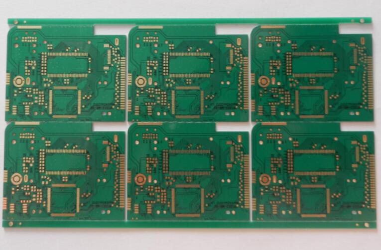
PCB layout
The first step in PCB production is to organize and check the PCB layout (Layout). The PCB production factory receives the CAD files from the PCB design company. Since each CAD software has its own unique file format, the PCB factory will convert it into a unified format Extended Gerber RS-274X or Gerber X2. Then the factory's engineers will check whether the PCB layout conforms to the manufacturing process, and whether there are any defects and other issues.
In the first issue of home-made PCB information, the PCB layout was printed on paper with a laser printer, and then transferred to the copper clad laminate. But in the printing process, because the printer is prone to lack of ink and breakpoints, it is necessary to manually fill up the ink with an oil-based pen.
Small-scale production is okay, but if this defect is transplanted to industrial production, it will greatly reduce production efficiency. Therefore, the factory generally uses photocopying to print the PCB layout on the film. If it is a multi-layer PCB board, the layout film photocopied for each layer will be arranged in order. Then the film will be punched with alignment holes. Alignment holes are very important. Afterwards, in order to align the materials of each layer of the PCB, the alignment holes must be relied on.
Production of core board
Clean the copper clad laminate, if there is dust, it may cause the final circuit to be short-circuited or broken.
Inner PCB layout transfer
Therefore, the two-layer circuit of the middle core board (Core) must be made first. After the copper clad laminate is cleaned, it will be covered with a photosensitive film on the surface. This film will solidify when exposed to light, forming a protective film on the copper foil of the copper clad laminate.
Insert the two-layer PCB layout film and the double-layer copper clad laminate, and finally insert the upper PCB layout film to ensure that the upper and lower PCB layout films are stacked accurately.

The photosensitive machine irradiates the photosensitive film on the copper foil with a UV lamp. The photosensitive film is cured under the light-transmitting film, and there is still no cured photosensitive film under the opaque film. The copper foil covered under the cured photosensitive film is the required PCB layout circuit, which is equivalent to the function of the laser printer ink of the manual PCB. In the paper PCB layout of the laser printer in the last issue, the copper foil to be kept under the black toner is covered. In this period, the copper foil covered by the black film will be corroded away, and the transparent film will be preserved due to the curing of the photosensitive film.
Then use lye to clean the uncured photosensitive film, and the required copper foil circuit will be covered by the cured photosensitive film.
Inner core board etching
Then use a strong base, such as NaOH, to etch away the unnecessary copper foil.
Tear off the cured photosensitive film to expose the copper foil of the required PCB layout.
Core board punching and inspection
The core board has been successfully produced. Then punch alignment holes on the core board to facilitate alignment with other materials.
Once the core board is pressed together with other layers of PCB, it cannot be modified, so inspection is very important. The machine will automatically compare with the PCB layout drawing to check for errors.
The first two layers of PCB boards have been made.
laminated
A new raw material is needed here called prepreg (Prepreg), which is the adhesive between the core board and the core board (the number of PCB layers>4), as well as the core board and the outer copper foil, and it also acts as an insulation.
The lower copper foil and the two layers of prepreg have been fixed in advance through the alignment hole and the lower iron plate, and then the finished core board is also placed in the alignment hole, and finally the two layers of prepreg, a layer of copper foil and A layer of pressure-bearing aluminum plate covers the core plate.
In order to improve work efficiency, this factory will stack three different PCB boards together before fixing them. The upper iron plate is magnetically attracted to facilitate alignment with the lower iron plate. After the two layers of iron plates are successfully aligned by inserting the alignment pins, the machine compresses the space between the iron plates as much as possible, and then fixes them with nails.
The PCB boards clamped by the iron plates are placed on the support, and then sent to the vacuum heat press for laminating. The high temperature in the vacuum hot press can melt the epoxy resin in the prepreg and fix the core boards and copper foils together under pressure.
After the lamination is completed, remove the upper iron plate that presses the PCB. Then remove the pressure-bearing aluminum plate. The aluminum plate also has the responsibility of isolating different PCBs and ensuring the smoothness of the outer copper foil of the PCB. Both sides of the PCB taken out at this time will be covered by a layer of smooth copper foil.
drilling
So how to connect 4 layers of copper foils that are not in contact with each other in the PCB? First, drill through the through-hole through the PCB, and then metalize the hole wall to conduct electricity.
Use the X-ray drilling machine to locate the inner core board. The machine will automatically find and locate the hole on the core board, and then punch the positioning hole on the PCB to ensure that the next hole is drilled from the center of the hole. pass.
Put a layer of aluminum plate on the punching machine machine, and then put the PCB on it. Since drilling is a relatively slow process, in order to improve efficiency, according to the number of layers of the PCB, 1 to 3 identical PCB boards are stacked together for drilling. Finally, cover the uppermost PCB with a layer of aluminum plate. The upper and lower layers of aluminum plate are used to prevent the copper foil on the PCB from tearing when the drill bit drills in and out.
Next, the operator only needs to select the correct drilling program, and the rest is done automatically by the drilling machine. The drill bit of the drilling machine is driven by air pressure, and the maximum rotation speed can reach 150,000 revolutions per minute. Such a high rotation speed is sufficient to ensure the smoothness of the hole wall.
The replacement of the drill bit is also automatically completed by the machine according to the program. The smallest drill bit can reach a diameter of 100 microns, while the diameter of a human hair is 150 microns.
In the previous lamination process, the molten epoxy was squeezed out of the PCB, so it needed to be cut off. The profiling milling machine cuts its periphery according to the correct XY coordinates of the PCB.
Chemical precipitation of copper on the hole wall
Since almost all PCB designs use perforations to connect different layers of lines, a good connection requires a 25-micron copper film on the hole wall. The thickness of the copper film needs to be realized by electroplating, but the hole wall is composed of non-conductive epoxy resin and glass fiber board. So the first step is to deposit a layer of conductive material on the hole wall, and form a 1 micron copper film on the entire PCB surface by chemical deposition, including the hole wall. The entire process such as chemical treatment and cleaning is controlled by the machine.
Fixing PCB-Cleaning PCB-Transporting PCB-Chemical Precipitation Copper Film
Outer PCB layout transfer
Next, the PCB layout of the outer layer will be transferred to the copper foil. The process is similar to the previous transfer principle of the inner core board PCB layout. The PCB layout is transferred to the copper foil by photocopying film and photosensitive film. The only difference is Yes, positive films will be used as the board.
Fix the printed PCB layout film of the upper and lower layers through the positioning holes, and put the PCB board in the middle. Then, the photosensitive film under the light-transmitting film is cured by the irradiation of the UV lamp, which is the circuit that needs to be reserved.
After cleaning off the unnecessary and uncured photosensitive film, inspect it.
Clamp the PCB with clamps, and electroplate the copper. As mentioned earlier, in order to ensure that the holes have sufficient conductivity, the copper film plated on the hole walls must have a thickness of 25 microns, so the entire system will be automatically controlled by the computer to ensure its accuracy.
Fixed PCB-computer control and copper electroplating
After the copper film is electroplated, the computer will arrange to electroplate a thin layer of tin.
After unloading the tin-plated PCB board, check to ensure that the thickness of the plated copper and tin is correct.
Outer PCB etching
Next, a complete automated assembly line completes the etching process. First, clean the cured photosensitive film on the PCB.
Then use a strong alkali to clean the unnecessary copper foil covered by it.
Then use the tin stripping solution to strip the tin plating on the PCB layout copper foil. After cleaning, the 4-layer PCB layout is complete.