Materials for high-density multilayer circuit boards
Multi-layer circuit boards have always been manufactured by through-hole plating. Since 1990, various build-up technologies have been proposed, and at the same time, many build-up process materials have been developed. Excluding special production methods, there are three types of more general build-up materials. They are photosensitive resin, thermosetting resin, and copper foil with resin. Other materials can also be integrated into three types of substrates according to the mode of operation. The first 70 is a comparison of some advantages and disadvantages of general high-density build-up circuit boards. Due to the gradual popularity of high-density build-up boards, not only the number of manufacturers but also the constant change of material properties, it is not necessarily appropriate to introduce specific products.
Each resin system will adjust its characteristics according to the process requirements, and its characteristics are from the basic resin monomer (Monomer) to 51, hardener (Hardener) 52, stabilizer (Stabilizer), additive (Additive), filler (Filler), etc. Matched. The demands of liquid resins are similar to those of solder resist inks, and the main focus is still on facilitating the coating to meet the characteristics of the final product. Vacuum laminated film is similar to ordinary dry film, but the resin must have the characteristics of a dielectric material. The hot-pressing type material should have the characteristic response of traditional film.
A photosensitive dielectric material
This type of material is mostly developed from a series of photosensitive solder resist products. Its micro-hole formation is completed by exposure to a negative film, and all micro-holes (vias) can be made at one time regardless of the hole density. Therefore, it is very promising in the early stage of the development of high-density build-up boards. After micro-hole processing, chemical copper and electroplated copper must be used to form circuit connections. In order to improve the adhesion to the chemical copper, the surface roughness must be made before the chemical copper to improve the bonding force of the copper. Since copper foil is not used, it will explore the use of full-board electroplating, full-etching process or semi-additive process (SAP-Semi Additive Process) to make the circuit.

Since photosensitive dielectric materials must take into account the physical properties and photosensitivity of the material, it is difficult to control the formulation of the material. There are two types of resins: liquid ink and film. Liquid products can be coated by screen printing, curtain coating, roller coating, etc. Because the flatness is not easy to control, the material characteristics, pressing or coating equipment, operating conditions, etc. must be properly controlled And choice.
Although the production cost of resin film is relatively high, it has greater advantages in terms of operation, thickness control, and cleanliness. Therefore, some products are also made in film form. Since the film is to be pressed on the uneven surface, the film is pressed by a vacuum laminator.
Photo-aperture technology is based on the image transfer of the hole position on the negative film, and the process of UV sensitization and development to make small holes. Developers vary with the resin system used, and there are two system products, alkaline aqueous solution and organic solvent. The environmental issues of aqueous systems are relatively minor, and solvent-based products are more troublesome, but some products still use solvent-based designs for the overall resin characteristics.
Two thermosetting resin materials
This type of resin will use carbon dioxide lasers or UV lasers for micro-hole processing, so the resin formulation does not need to consider photosensitivity. The relative flexibility of the resin is wider, and the physical properties of the product are relatively easy to achieve. Generally, the characteristic requirements of this kind of resin system mainly focus on the characteristics of laser light absorption, fluorescence reflection characteristics, chemical resistance, and coarsening applicability.
This type of resin products are divided into liquid ink and film. After coating or laminating, laser drilling is performed, and then interlayer conduction and circuit production are performed by electroplating. Since there is no surface copper, it must be treated with chemical copper as a seed layer for electroplating. In order to ensure the bonding force between the copper and the resin, the resin surface must be roughened to obtain the anchor force. Generally, the tensile force that can be achieved is about 0.8 to 1.2 kg/cm.
The basic coating method of the liquid resin is the same as that of the photosensitive resin, and the film type material is also similar to the photosensitive type. Generally, the film thickness of a high-density build-up circuit board is usually distributed between 40~80 // m. Because there is no copper skin on the board, no matter it is photosensitive or thermosetting resin, the etching amount is less, which is beneficial to the production of fine lines.
Three with resin copper skin material, or back glue Copper skin
This type of material is mainly developed to comply with the traditional circuit board manufacturing mode, which is to coat B-stage thermosetting resin on the roughened surface of the copper skin. The thickness of the copper skin used is generally 12 # m or 18 // m, which is more, but ultra-thin copper skin is used for special purposes. The thickness of the resin must be determined according to the requirements of the filling amount, and the thickness after pressing is generally used as an index.
Due to the copper skin pressing process, the bonding force comes from the adhesion of the resin melting and the copper skin, and the copper skin pulling force is relatively stable and similar to traditional circuit boards. The use of thermocompression technology and traditional stacking methods has better compatibility in the tools and operations used, and the easy introduction of the manufacturing process is the reason why it is widely used, and many manufacturers have put into production.
In the early stage of the development of high-density build-up boards, this type of material will use image transfer and etching to open a copper window (Conformal Mask) on the copper foil, so this type of process is called the Conformal mask method. A few years later, due to the advancement of laser technology and the gradual maturity of process technology, some processes also began to explore the mode of laser direct processing, so this type of process is called LDD-Laser Direct Drill Note 53 method. Due to the shielding of copper, the entire board surface after the build-up is covered by copper foil. How to make reference identification is a problem that must be faced. This is the so-called tool system compatibility, which must be considered during production and design. .
Such materials still have to rely on etching when making circuits, and the amount of etching is much larger than that of circuit boards without copper, which is not conducive to the control of circuit accuracy. This is why many copper sheet manufacturers have recently invested in the development and production of thin copper sheets.
Four other types of materials
Of course, the materials used in high-density build-up circuit boards are not limited to those mentioned above, and products of different shapes are still being used or developed. For example, some products are not satisfied with the structure without reinforcing fiber, but adding fiber is not conducive to processing. Therefore, in order to improve the physical characteristics of the circuit board, a special flat glass fiber material is used to make the laser processing layer. At this time, not only the pressing process and the expansion and contraction design must be reconsidered, but also the laser processing conditions must be re-adjusted.
As for the well-known ALIVH process, the film is made of Aramid fiber non-woven fabric impregnated with resin, which makes it easier for laser processing.
B2IT uses silver paste to form bumps to penetrate the film, and then bond it with copper by pressing. Therefore, the silver paste used is special and there are fewer restrictions on the choice of film.
The American Goretex company uses PTFE fiber to make fibrous film, because the use of PTFE can reduce the dielectric constant, so it is conducive to high-speed transmission products.
Five high-frequency material trends
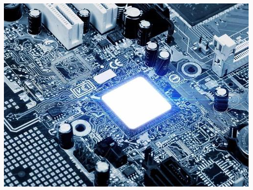
From the evolution of personal computers, it can be seen that the speed of CPU generations is getting faster and faster, and consumers are overwhelmed. Of course, it is a good thing for the public. But it is a further challenge to PCB production. Because of the high frequency, it is necessary for the substrate to have lower Dk and Df values.