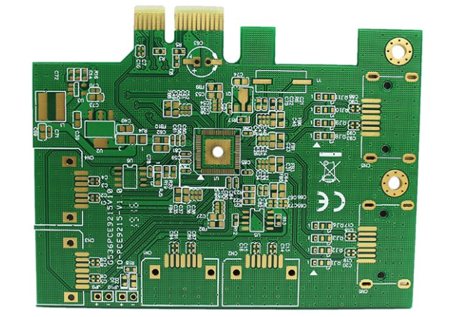
Classification and technology of high-density circuit boards
A multi-layer printed circuit board with through-hole plating
Through-hole plating has been used in multilayer printed circuit boards for more than 20 years. To understand the circuit board industry, the knowledge of through-hole plating is a basic task for circuit board manufacturers.
The through-holes of the circuit board generally provide two functions, namely, conducting interlayer circuits and installing through-hole components. If it is a through hole purely for conduction, there is a more commonly used term in English called (Via), which is not exactly the same as a hole (Hole) in meaning, but the meaning of Chinese characters is called a hole, so there is The so-called part hole is different from the via hole. In order to increase the density of the circuit board, reduce the number of layers, and facilitate assembly, surface-mounted electronic components are used in large quantities. Except for specific terminals and tool holes, which are designed with large apertures, almost all holes that are purely conductive are used as much as possible. The smallest hole design is used to reduce the occupied area.

Usually most circuit boards will not explore all the structures at once. The through-hole structure is a necessary structure for the assembly of through-hole components. Other holes are only made to increase the wiring density. The higher the density, the greater the number of layers, and the thinner the thickness of the interlayer, the more difficult it is to make.
In order to avoid the waste of a lot of winding space in the traditional structure where all the through holes are from the beginning to the end, the board structure shown in Figure 1 is made using part of the surface through hole pattern. This structure can make full use of the three-dimensional space at the same location. And there is no shortcoming of low space utilization of traditional circuit boards. Since the surface through-hole pressing board has been filled with resin, the surface holes become flat copper pads after subsequent electroplating treatment, which can directly mount electronic components, which is beneficial to increase the density.
Two metal core board and soft and hard board
Circuit boards designed for special purposes are different from general multi-layer circuit boards. For example, metal core boards designed for high power consumption, high temperature and high heat equipment are an example.
The metal core board disposes thicker metal in the area of high heating element, and the power supply directly exposes the metal block to directly contact the element. Some designs only explore the use of thicker copper skin for partial heat dissipation improvement, so it is common The thickness of the copper skin is about 0.5? 2 oz, and its structure still maintains a double number. However, the metal core board particularly emphasizes the heat dissipation efficiency. The commonly used metal thickness is about 3-14oz. Because of the addition of a thick metal layer, the total number of metal layers is often singular, which is very different from general circuit boards. Although the metal core board has its complexity in the production process and design, it still has its own value for high-power equipment and components.
Rigid and flexible boards made of a combination of rigid boards and flexible boards are mainly to meet the requirements of performance improvement, lighter weight, and space saving. It can avoid the trouble of connector wiring, but the cost is higher due to the troublesome production process. In addition to military and aerospace applications, general electronic products are more likely to be used, such as display modules, etc., traces of such circuit boards can be seen .
Three high-density build-up printed circuit boards
The high-density build-up printed circuit board is a circuit board made by the sequential construction of the circuit layer and the insulating layer process. In the early stage of the development of high-density circuit boards, the designed structure is based on the resin without reinforcing materials as the insulating substrate of the high-density layer. Therefore, the design method is based on the traditional rigid board structure, and then builds pure resin high-density on it.的线. The line. Of course, some circuit boards adopt different methods and do not follow the structure with a thicker substrate in the middle. Such a structure is called Core-less technology, and the ALIVH developed in Japan is classified as this type of technology.
Because the traditional circuit board structure is not easy to make tiny holes, so there are developers who use image transfer, laser technology or other hole-forming methods to make small holes, which can save copper pads (Pad) Configure space, reserve more space to make winding easier, and because the insulating layer becomes thinner, the characteristic impedance and electromagnetic effect are also better.
Four transfer method high density printed circuit board
The definition of high density means that more copper pads and connecting lines can be configured in the same plane space, so the technology that can make fine lines, small holes, and high cumulative density can be classified as high-density circuit board technology.