Application areas of multilayer circuit boards
Multi-layer PCBA board generally use plated through holes as the core, and the number of layers, board thickness, and hole configuration vary with the line density. Most of the classification of its specifications is based on this. Rigid-Flex is mostly used in military, aerospace and instrument equipment, and is rare in general consumer electronics products. Therefore, it will not be discussed in detail. Under the precondition that electronic products tend to be multi-functional and complex, the contact distance of integrated circuit components has been reduced, and the speed of signal transmission has been relatively increased. This is followed by an increase in the number of wiring and the length of wiring between points. The performance is shortened, and these require high-density circuit configuration and microvia technology to achieve the goal. Wiring and jumper are basically difficult to achieve for single and double panels, so the circuit board will be multi-layered; and because of the continuous increase of signal lines, more power layers and grounding layers have become necessary means for design All of these have made Multilayer Printed Circuit Board (Multilayer Printed Circuit Board) more common.
Ways of connecting multiple layers
The printed circuit board builds the metal layer on an independent circuit layer, so the vertical connection between the layers is indispensable. In order to achieve the purpose of interlayer connection, it is necessary to use a drilling method to form a via and form a reliable conductor on the hole wall to complete the connection of power or signal. Since through-hole plating was proposed, almost all multilayer circuit boards have been produced using this method. |
The increased-density circuit board explores the build-up manufacturing mode, which is formed by forming small holes in the dielectric material in a laser or light-sensing manner, and then conducting it by electroplating. Some manufacturers use conductive glue to fill the connecting holes to achieve conduction. The ALIVH, B2it, etc. developed in Japan fall into this category.

Sectional geometry of multilayer circuit boards
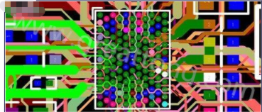
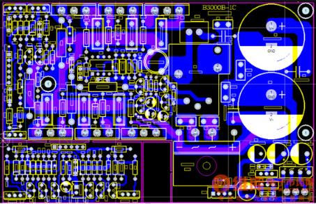
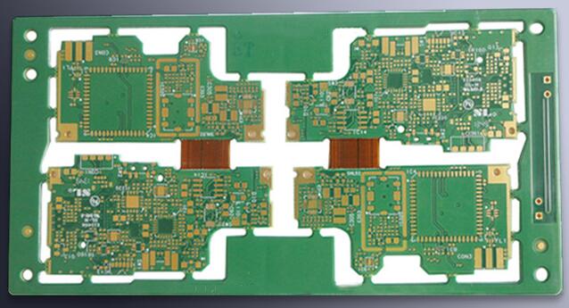
Multilayer printed circuit boards will have single-sided, double-sided, 4-layer, 6-layer, 8-layer, etc. structures depending on the number of layers of the circuit. As for the high-density circuit boards that are often mentioned recently, because the usual manufacturing method is to build a core hard board in the center, and use this as a basis to grow and increase the layers on the upper and lower sides. Therefore, there are two common names. One is to use the number of hard board layers in the center as the first number, and the number of wire layers added on both sides as the other number, so there are so-called descriptions of 4+2, 2+2, 6+4, and so on. But another name may be easier for people to understand the actual situation, because most multi-layer circuit board designs use symmetrical design, so the names 1+4+1, 3+6+3, etc. are used. At this time, if Some people say that a 2+4 structure may be an asymmetric structure, and it must be confirmed.
ipcb is a high-precision, high-quality PCB manufacturer, such as: isola 370hr PCB, high-frequency PCB, high-speed PCB, ic substrate, ic test board, impedance PCB, HDI PCB, Rigid-Flex PCB, buried blind PCB, advanced PCB, microwave PCB, telfon PCB and other ipcb are good at PCB manufacturing.