Cause analysis and prevention of PCBA assembly explosion-PCB with CTI parameter requirements
To figure out the use of high CTI special printed boards, you must first understand CTI and its principles, copper clad laminates and PCB manufacturing processes.
CTI and its principle
CTI refers to the relative leakage index or the relative tracking index. It refers to the highest voltage value at which the surface of the PCB substrate can withstand 50 drops of electrolyte without forming a leakage hum. This value must be a multiple of 25, according to IEC -112 standard test.
When the surface of the copper clad polymer solid insulating material substrate is polluted by solution pollutants with positive and negative ions, when a certain voltage is applied, the leakage current on the surface is much larger than that of the clean surface. According to the heat formula Q= The square of R*I. When the leakage current increases, the heat generated by the leakage current increases, and the rate of evaporating wet pollutants increases. This is an uneven dry state formed on the surface of the polymer material, which leads to the formation of a dry zone or dryness on the surface of the polymer material. point. The dry zone increases the surface resistance, so that the electric field becomes non-uniform, which in turn produces flashover discharge points. Under the combined action of electric field and heat, the surface of the insulator material is promoted to talk, and the resistance of the carbide is small, which promotes the increase of the electric field intensity formed by the click tip of the applied voltage, and therefore it is easier to produce a flashover discharge point. Such a vicious circle, it is known that the surface resistance between the electrodes that cause the applied voltage is destroyed, forming a conductive channel, and causing leakage tracking.

Once the copper clad laminate polymer solid insulation material substrate has leakage tracking, there will be three kinds of deterioration phenomena. One is a carbonized black dendritic conductive channel. After multiple consecutive placements, the conductive channel continues to grow. When the two poles are bridged When connected, the material can be broken down; but under the action of multiple points, the material catches fire and is destroyed; third, there are some pits in the material, and when the point continues to go on, the pits deepen and generate electricity. Corrosion, the advantage occurs click-through damage, and sometimes it is not broken down.
According to the International Electrotechnical Commission 664A, 950 standards and UL standards, insulation materials are divided into six grades according to the CTI value.
Design choice for CT
Leakage traces, a simple summary description is the process of the polymer solid insulating material gradually forming a conductive path under the combined action of the electric field and the electrolyte. The ability of solid polymer insulation materials to resist tracking is called tracking index CTI.
Among the many properties of copper clad laminates, the tracking resistance performance parameter, as an important safety and reliability index, has been paid more and more attention by PCB designers and complete circuit board manufacturers. Copper clad laminates with low CTI values are at high pressure and high temperature. Long-term use in harsh environments such as damp, dirty, etc., is prone to leakage tracking. Under continuous leakage damage, the insulation layer will sometimes become a short circuit due to the carbonization of the substrate material, which affects the safe service life of electronic and electrical products. Generally, the good CTI of ordinary paper-based copper clad laminate is less than 150, and the CTI of ordinary copper clad laminate and ordinary glass fiber cloth-based copper clad laminate is 175~225, which can not meet the higher safety requirements of electronic and electrical products. In the IEC-950 standard, the relationship between the CTI of the copper clad laminate and the working voltage of the PCB and the minimum wire distance are stipulated. The high CTI value of the copper clad laminate is not only suitable for use in harsh environments such as high pressure, high temperature, humidity, and pollution, but also It is very suitable for making high-density PCB, because the line spacing of PCB made with high CTI value of copper clad laminate can be allowed to be smaller.
As people have higher and higher requirements for the safety and reliability of electronic and electrical products, the use environment of electronic and electrical products is getting worse and more uncertain, especially if it is required to be used in high pressure, high temperature, humidity, and pollution. The PCB design of electronic and electrical products must have requirements for electrical tracking resistance CTI. Safety and reliability are an important factor in the quality assurance of electronic and electrical products. PCB is the basis of the product. PCB design should select a printed board substrate with a suitable CTI value according to the needs.
Production of high CTI copper clad laminate
From the above conductive trace principle, it can be seen that there is a problem with this high CTI special copper clad laminate, which causes serious failures in subsequent use, and the quality of the production and production of the copper clad laminate must be monitored.
Based on high CTI requirements, the manufacture of copper clad laminates must use epoxy resin and inorganic fillers with excellent tracking resistance to produce PCB boards with CTI>600. This kind of copper clad laminate is a multi-layer laminate, and the performance of the board must meet the IPC-4101 standard.
The composition of this copper clad laminate is mainly organic materials such as epoxy resin and its cured products, and inorganic materials such as glass fibers. The composition of the glass fiber is Lv Peng silicate, which is an inorganic substance and will not be carbonized and traced. The organic matter such as epoxy resin and its cured products is the fundamental factor for the tracking of the board. Among them, low-halogen or halogen-free epoxy resin plays a decisive role in improving the CTI value. In the manufacturing process of copper clad laminates, the control of the amount of inorganic fillers also has a certain effect on improving CTI.
The production process of the board is as follows: the synthesis and configuration of resin glue (gluing)-fiberglass cloth dipping-dipping fiberglass cloth drying-prepreg cutting-lamination-pressing plate forming (the hotter- -Hot pressing-cooling)-shearing-packaging. That is, the main process is to use glass fiber cloth impregnated with epoxy resin, curing agent, aluminum hydroxide, and high-efficiency flame retardant as the main glue to make high CTI fabrics, and glass fiber paper is impregnated with epoxy resin, curing agent, The glue with the filler as the main body is dried to make the core material, which is superimposed in the order of high CTI fabric + core material (the number of core materials depends on the thickness of the board) + high CTI fabric, and copper foil is placed on the measuring surface, and then placed Into the hot press, heat and press to make a copper clad laminate with high CTI value.
The base material for multilayer PCB is composed of copper foil, prepreg, and core board. Below is the CTI test comparison curve of common copper clad laminate CEM-3 and copper clad laminate S2600 with CTI>600.
From the perspective of the manufacturing technical performance of CTI.>600 copper clad laminates, the thermal stress index of the copper clad laminate is required to be free of delamination and no blistering under the experimental conditions of 260 degrees Celsius and 20s. It can be seen that for the manufactured PCB, after the normal reflow soldering and wave soldering, the explosion of the plate is the cause of the plate.
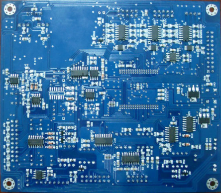
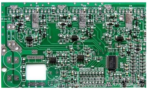
PCB production with CTI>600
The high CTI value of the copper clad laminate must be strictly inspected before use. In the manufacturing process of the high CTI value of the PCB, the copper clad laminate is first cut, and then the cut copper clad laminate is baked. Although this process is a common process for PCB manufacturing, it is particularly important in the production of PCBs with high CTI values.
The process of baking the board is the preheating and dehumidification treatment, that is, the copper clad laminate is baked in a high temperature oven for a period of time (note that the board cannot directly contact the heat source). The temperature and time of the baking sheet need to be determined according to the thickness, area and quantity of the sheet, usually between 120 and 130 degrees Celsius. When laminating boards, prevent debris, dust, etc. from entering between the boards, and the temperature of the preheating and dehumidification treatment must not be too high, because too high temperature will cause the copper clad laminate to warp. When the moisture-absorbing copper clad laminate is processed for moisture removal, if the temperature rises too quickly, the water in the material will expand, which will cause quality problems such as white spots and interlayer cracking (ie, bursting) of the board.
The purpose of the baking board is to reduce the residual internal stress of the copper clad laminate, remove the moisture in the board, and improve the warpage deformation generated during the PCB manufacturing process.
The PCB processing and production process is as follows: cutting board-baking-inner layer graphics transfer (filming-exposure-development-etching-removing film)-lamination (stacking-pressing)- -Mechanical drilling-metallization hole-outer layer pattern transfer (filming-exposure-development)-pattern plating (copper plating + tin plating)-outer layer etching (film removal-etching-stripping tin )-Photosensitive solder mask-surface treatment-baking-packaging.
In the process of PCB processing, such as hole processing, hole metallization, graphic production, character printing, etc., there will be problems with heating the board. During the processing, the board is heated by moisture absorption (including absorption of organic solvents, water, etc.). If the heating conditions are not properly controlled, problems such as delamination of the board, white spots, peeling of copper foil, blistering, and warping will occur. . Therefore, it is necessary to strictly control the heating conditions of each processing procedure in the PCB production process to prevent defects due to thermal stress. This is also the difficulty in the production of this special PCB with high CTI value, which cannot be produced by any printed circuit board manufacturer. .
After the PCB manufacturing process is completed, an important process is to carry out the baking process to increase the sealing of the printed board packaging, and finally put a desiccant in the large package.