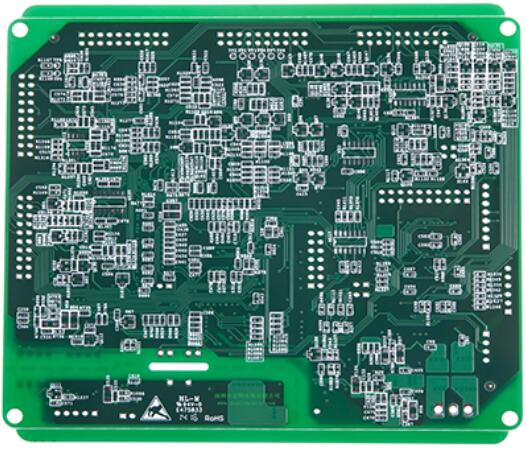
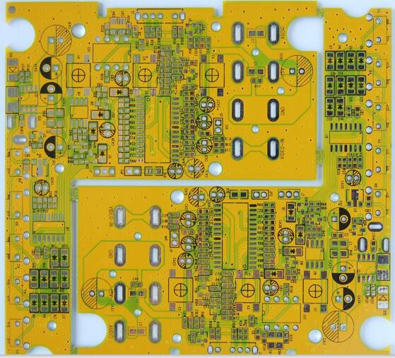
PCB board flying probe test introduction
Flying probe test is one of the methods to check the electrical function of PCB (open and short circuit test). The flying tester is a system for testing PCBs in a manufacturing environment. Instead of using all the traditional bed-of-nails interfaces on traditional online testing machines, flying probe testing uses four to eight independently controlled probes to move to the component under test.

The unit under test (UUT, unit under test) is transported to the testing machine through a belt or other UUT conveying system. Then it is fixed, the probe of the tester contacts the test pad (test pad) and the via hole (via) to test a single component of the unit under test (UUT).
The test probe is connected to the driver (signal generator, power supply, etc.) and sensor (digital multimeter, frequency counter, etc.) through a multiplexing system to test the components on the UUT. When a component is being tested, other components on the UUT are electrically shielded by the prober to prevent reading interference.
The difference between flying probe test and test stand test
Flying probe test: It uses 4 probes to conduct high-voltage insulation and low-resistance continuity test (testing the open circuit and short circuit of the circuit) on the circuit board without the need for test fixtures. Directly install the PCB board and run the test program to test extremely It is convenient, saves the cost of testing, reduces the time for making test racks, improves the efficiency of shipping, and is suitable for testing small batches and prototypes.
The test rack is a special test fixture for on-off testing of mass-produced PCB boards. The production cost is relatively high, but the test efficiency is better, and there is no charge for returning the order. The two test methods are different, and the equipment is also different.
Introduction to hot air leveling of PCB boards
Hot air leveling, also known as hot air solder leveling (commonly known as spray tin), is a process of coating molten tin (lead) solder on the surface of the PCB and flattening (blowing) it with heated compressed air to form a layer that is resistant to copper oxidation. It can also provide a coating layer with good solderability.

During hot air leveling, solder and copper form a copper-tin intermetallic compound at the junction. When the PCB is leveled with hot air, it should be submerged in the molten solder; the air knife blows the liquid solder before the solder solidifies; the air knife can minimize the meniscus of the solder on the copper surface and prevent the solder from bridging.
Advantages of hot air leveling process
(1) After hot air leveling, the composition of the solder coating remains unchanged, so that the solder coating has good consistency and excellent solderability. As for the lead-tin alloy coating obtained by electroplating, the composition (the ratio of lead to tin) changes with the change of the composition in the plating solution.
(2) Neither the infrared fusion process nor the hot oil fusion process can protect the side edges of the wire 100%. The solder coating that is leveled by hot air can completely cover the side edges of the wires, avoid corrosion and disconnection on the printed board, extend the storage and use time of the printed board, and improve the reliability of the electronic products of the whole machine. Hot air leveling is now widely used in the SMT process.
(3) By adjusting the air knife angle, the rising speed of the printed board and other process parameters, the coating thickness can be controlled to obtain the required solder coating thickness, which is more convenient and flexible than thermal melting.
(4) The printed boards produced by pattern plating and etching are prone to bridging due to the lead-tin alloy on the wires during wave soldering. In the same way, the flow of the lead-tin alloy causes the solder mask to wrinkle and warp. The printed boards produced by the hot air leveling process have no solder on the wires, which eliminates solder bridging, wrinkling and shedding of the hindered film.
Disadvantages of hot air leveling process
(1) Contamination of the solder bath by copper. When leveling with hot air, the printed board must be immersed in the solder bath for a few seconds, causing the copper to dissolve. When the copper concentration reaches more than 0.29%, the fluidity of the solder becomes poor, the coated solder layer is in a semi-wetting state, and the solderability of the printed board decreases.
(2) In the solder coating, lead is a heavy metal element, which is harmful to the human body and pollutes the environment. Now some lead-free solders have been produced and sold instead of lead-tin alloys for production.
(3) The production cost is high. An imported and better hot-air leveling machine sells for more than US$300,000, so its production cost is higher than that of the hot-melt process.
(4) The hot air leveling has a large thermal shock, which is easy to deform and warp the printed board. The thermal stress is large.