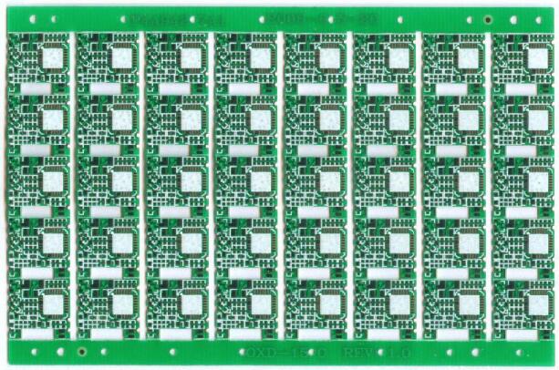
PCB etching introduction
The process of the PCB from the light board to the circuit pattern is relatively complicated. The current typical process of the circuit board (PCB) processing adopts the "pattern plating method", that is, the copper foil part that needs to be retained on the outer layer of the pring circuit board, that is, the circuit The pattern part is pre-plated with a layer of lead-tin anti-corrosion layer, and then the remaining copper foil is etched away by chemical means, which is called etching.

Causes of side erosion
1, etching method
Soaking and bubbling etching will cause larger side etching, splashing and spray etching are smaller, especially spray etching has the best effect.
2, the type of etching solution
Different etching solutions have different chemical components, their etching rates are different, and the etching coefficients are also different. For example, the etching coefficient of an acidic copper chloride etching solution is usually 3, and the etching coefficient of an alkaline copper chloride etching solution can reach 4. Recent studies have shown that an etching system based on nitric acid can achieve almost no side etching, and the sidewalls of the etched lines are nearly vertical.
3, etching rate
Slow etching rate will cause severe side etching, and the improvement of etching quality has a great relationship with the acceleration of etching rate. The faster the etching speed, the shorter the time the board stays in the etching solution, the smaller the amount of side etching, and the etched patterns are clear and neat.
4. PH value of etching solution
When the pH value of the alkaline etching solution is higher, the side corrosion will increase. In order to reduce the side corrosion, the PH value should generally be controlled below 8.5.
5. Density of etching solution
The density of the alkaline etching solution is too low, which will increase the side etching. The selection of an etching solution with a high copper concentration is beneficial to reduce the side etching.
6, copper foil thickness
For the etching of thin wires with minimal undercutting, it is best to use (ultra) thin copper foil. And the thinner the line width, the thinner the copper foil thickness should be. Because the thinner the copper foil, the shorter the time in the etching solution, the smaller the amount of side etching.
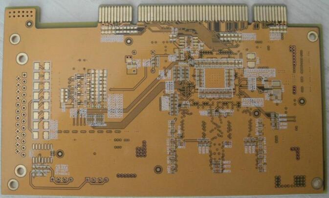
PCB board gold finger introduction
Golden Finger: (Gold Finger or Edge Connector) Insert one end of the PCB into the connector card slot, use the connector pin as the outlet of the PCB board to connect to the outside, so that the pad or copper skin is in contact with the pin at the corresponding position To achieve the purpose of conduction, and nickel-gold plated on this pad or copper skin of the circuit board, it is called a gold finger because it is in the shape of a finger.

The reason why gold was chosen is because of its superior conductivity, oxidation resistance, and wear resistance. However, because of the high cost of gold, it is only used for partial gold plating such as gold fingers.
PCB board gold finger types
1, conventional gold finger (flush finger)
Rectangular pads with the same length and width are arranged neatly on the edge of the board.
2, long and short golden fingers (i.e. uneven golden fingers)
Rectangular pads with different lengths located at the edge of the board.
3, segmented cheats (intermittent cheats)
Rectangular pads with different lengths located at the edge of the board, and the front section is disconnected.
PCB board gold finger features
There is no character frame and label, and it is usually a solder mask opening window. Most of the shapes have grooves, and the gold finger part protrudes from the edge of the board or is close to the edge of the board. Some boards have gold fingers on both ends, normal gold fingers have both sides, some PCB circuit boards have only single-sided gold fingers, and some PCB boards have a single gold finger that is wider.