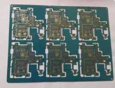
OSP circuit board introduction
OSP is a process for surface treatment of printed circuit board(PCB) copper foil that meets the requirements of the RoHS directive. OSP is translated as organic solder protection film, also known as copper protection agent. Simply put, OSP is to chemically grow a layer of organic film on the clean bare copper surface.

This layer of film has anti-oxidation, thermal shock resistance, and moisture resistance to protect the copper surface from rusting (oxidation or sulfidation, etc.) in a normal environment; but in the subsequent welding high temperature, this kind of protective film must be very It is easy to be quickly removed by the flux, so that the exposed clean copper surface can be immediately combined with the molten solder into a strong solder joint in a very short time.
OSP circuit board storage requirements
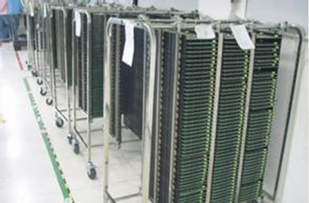
When the preservative produced by OSP technology is too thin and easy to cut, you must be very careful during handling and transportation. The PCB with OSP surface finish is exposed to high temperature and high humidity for so long that oxidation may occur on the surface of the PCB, resulting in low solderability. Therefore, the storage method must follow the following principles:
1. Vacuum packaging should be used together with desiccant and humidity display card. Place release paper between PCBs to prevent friction from damaging the PCB surface.
2. These PCBs cannot be directly exposed to sunlight. The requirements for the best storage environment include: relative humidity (30-70%RH), temperature (15-30°C) and storage time (less than 12 months).
Why do impedance
1. The PCB board should consider plugging and installing electronic components. After plugging, the conductivity and signal transmission performance should be considered. Therefore, the lower the impedance, the better, and the resistivity should be less than 1&TImes;10-6 per square centimeter.
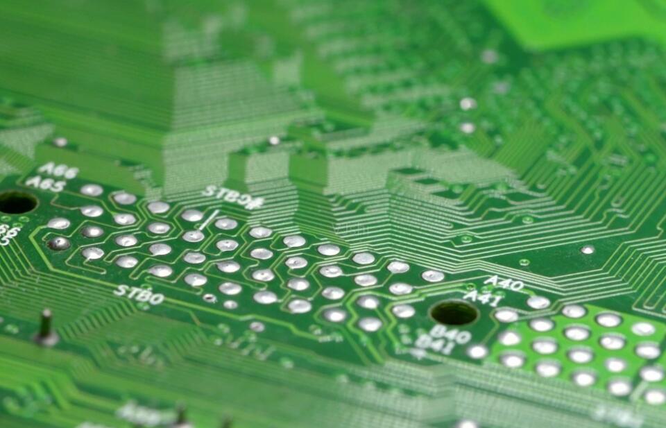
2. In the production process, it is necessary to go through the process of copper sinking, electrolytic tin (or electroless plating, or thermal spray tin), connector soldering, etc., and the materials used in these links must ensure the low resistivity to ensure the PCB board The overall impedance is low to meet the product quality requirements, and it can operate normally.
3, tinning is the most prone to problems in the production of the entire circuit board, and it is the key link that affects the impedance. The biggest defect of the electroless tin coating is easy discoloration (both easy to oxidize or deliquesce) and poor solderability, which can lead to difficult soldering of the PCB board, high impedance, poor electrical conductivity, or instability of the overall board performance.
4. There are various signal transmissions in the conductor. When it is necessary to increase its frequency in order to increase its transmission rate, if the line itself is different due to factors such as etching, stack thickness, wire width, etc., the impedance value will change and the signal will be distorted., Resulting in a decrease in the performance of the PCB board, so it is necessary to control the impedance value within a certain range.

Causes of high impedance
1. The lines of the PCB board are relatively thin, which leads to higher resistance of the PCB board.
2. The copper thickness of the PCB board is relatively thin, which leads to higher resistance of the PCB board.
3, the line spacing of the PCB board, the thickness of the dielectric layer is too thick, and the thickness of the outer ink is too thick, which causes the resistance of the PCB board to become higher.