The width of PCB process edge setting standard
Printed circuit boards{Printed circuit boards}, also known as printed circuit boards, are providers of electrical connections for electronic components.
Printed circuit boards are often represented by "PCB", but cannot be called "PCB boards".
Its development has a history of more than 100 years; its design is mainly layout design; the main advantage of using circuit boards is to greatly reduce wiring and assembly errors, and improve the level of automation and production labor rate.
According to the number of circuit boards, it can be divided into single-sided boards, double-sided boards, four-layer boards, six-layer boards and other multilayer circuit boards.
Since the printed circuit board is not a general terminal product, the definition of the name is slightly confusing. For example, the motherboard for personal computers is called the motherboard, and cannot be directly called the circuit board. Although there are circuit boards in the motherboard, They are not the same, so when evaluating the industry, the two are related but cannot be said to be the same. Another example: because there are integrated circuit components mounted on the circuit board, the news media call it an IC board, but in fact it is not equivalent to a printed circuit board. We usually say that the printed circuit board refers to the bare board-that is, the circuit board without upper components.

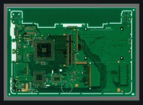
In the PCB process, the reservation of the process edge is of great significance for the subsequent SMT chip processing. The process side is to assist in the production of the plug-in board, the part of the welding wave on the two or four sides of the PCB board. It is mainly used to assist the production. It is not part of the PCB board and can be removed after the manufacturing is completed. The main reason for leaving the process side is that the SMT placement machine track is used to clamp the PCB board and flow through the placement machine, so the components that are too close to the track side are picked up by the suction nozzle of the SMT placement machine and mounted to When the PCB board, the phenomenon of collision occurs, and the production cannot be completed, so a certain process edge must be reserved, such as 2~5mm and so on. The same applies to some plug-in components to prevent similar phenomena during wave soldering.
Since the process side consumes more PCB plates and increases the overall cost of the PCB, it is necessary to balance economy and manufacturability when designing the PCB process side. For some special-shaped PCB boards, the original PCB board with 2 process edges or 4 process edges can be greatly simplified through the method of splicing. When designing the splicing method, it is necessary to fully consider the track width of the SMT placement machine. For splicing with a width of more than 350mm, it is necessary to communicate with the process engineer of the SMT supplier.
The flatness of the PCB process edge is also an important part of the PCB production, which has a big relationship with V-Cut. When removing the PCB process edges, it is necessary to ensure that the process edges are flat, especially for PCBs that require extremely high assembly accuracy. Any uneven burrs will cause the mounting holes to shift and cause great troubles for subsequent assembly.