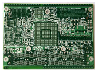
When the PCB factory designs the circuit board, the circuit principle design is very good, or even very good. However, various noises will appear during the debugging process. The circuit board cannot achieve the expected purpose, and sometimes it is even worse. Relay the board. So how can we reduce the noise of the circuit board? The analysis is as follows:
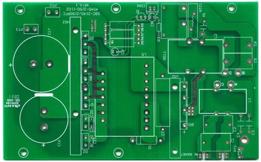
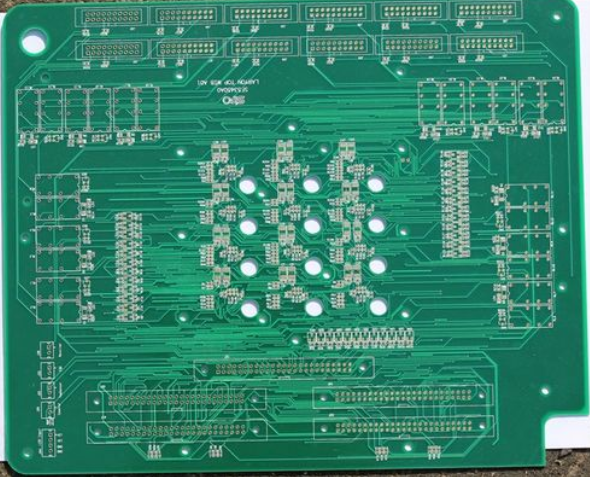
A board with good performance, the circuit board designer can see its general distribution at a glance (provided that the board knows what function the board is), this is the principle of separation of functional modules we often say. A functional module is a collection of circuits that have some electronic components combined to complete a certain function. In actual design, we need to put these electronic components close to reduce the wiring length between the electronic components in order to increase the role of the circuit module. In fact, this is not difficult to understand. Our common development boards or mobile phones do this, especially mobile phones. If you disassemble the mobile phone, you will find that the separation between the various modules is obvious, and each module is Faraday The electric cage is shielded.

Secondly, it should be noted that when there are analog and digital circuits on a PCB circuit board, the two need to be separated. If you have to buckle a hat, there will be a quiet zone. The so-called quiet zone is the area that physically separates analog circuits and digital circuits or various functional modules. In this way, you can prevent other modules from interfering with the module. In the mobile phone circuit board mentioned above, the quiet zone is obvious. Note that the quiet zone and the circuit board ground are not connected.
In the actual circuit board design, not every PCB board has enough space for us to make a quiet zone. Then, when the space is not allowed, how should we design?
A. Use transformers or signal isolation components for design. We often use CMOS or transistors and other components to form a circuit separation that is the meaning.
B. The signal passes through the filter circuit before entering the module. This method is a common method to prevent ESD. Putting it here is also considering that this method can play a role in eliminating noise (ESD, high frequency and high voltage noise).
C. Use common mode inductors for signal protection. If you don't know the role of common mode inductance, we will find in the schematic diagram that there are only two coils, which have no effect. In fact, this is not the case, it plays an important role in the stability of the signal and the elimination of noise interference. This also reveals on the other hand that electronic engineers need long-term training to grow.
A method similar to the quiet zone of circuit board design is trench protection technology. This technique is to remove the divided copper skin in the quiet zone to form a bare circuit board material. The concept of the bridge is also derived from this: the power, ground and signal traces that connect the various sub-zones together are called bridges. The trench protection technology has the ability to withstand the impact of peak voltage and classic discharge protection, which can reduce the noise of the circuit board to a certain extent. In the circuit board design, when the wiring that has nothing to do with the isolation area passes through the protective trench, RF loop current will be generated, which will further affect the performance of the circuit board. This requires attention.
Now, many analog-to-digital or digital-to-analog components have connected the two parts of the ground together inside the component, typically ADC and DAC devices. These devices must have a standard reference ground if the digital signal current Failure to return to the source effectively will cause noise to generate EMI. When drawing the schematic, we found that the pins with AGND and DGND are a device with superior performance, which will reduce the difficulty of our design.
In general, during the PCB manufacturing process, the circuit should be partitioned according to the modules. The obvious quiet zone between the partitions is to minimize the influence of the power and ground on the signal and minimize the noise of the circuit board. Reduce to a minimum.