With the development of the electrical age, there are more and more electromagnetic wave sources in the human living environment, such as radio broadcasting, television, microwave communications, household appliances, power frequency electromagnetic fields and high frequency electromagnetic fields of power transmission lines. When the field strength of these electromagnetic fields exceeds a certain limit and the action time is long enough, they may endanger human health; at the same time, they may also interfere with other electronic equipment and communications. In this regard, protection is required. The concepts of electromagnetic interference and shielding are often put forward during the development, production, and use of electronic products. When electronic products are operating normally, the core is a coordinated working process between the PCB board and the components and parts installed on it. It is very important to improve the performance index of electronic products and reduce the influence of electromagnetic interference.
Printed circuit board (PCB) is the support of circuit components and devices in electronic products. It provides electrical connections between circuit components and devices. It is the most basic component of various electronic equipment. The performance of PCB boards is directly related to The quality and performance of electronic equipment. With the development of integrated circuits, SMT technology, and micro-assembly technology, there are more and more high-density, multi-functional electronic products, resulting in complex wire layout on PCB boards, numerous parts and components, and dense installation, which will inevitably cause interference between them It is getting more and more serious, so the problem of suppressing electromagnetic interference has become the key to whether an electronic system can work normally. Similarly, with the development of electrical technology, the density of PCB is getting higher and higher, and the quality of PCB board design has a great influence on the interference and anti-interference ability of the circuit. In order to obtain the best performance of electronic circuits, in addition to the selection of components and circuit design, good PCB board design is also a very important factor in electromagnetic compatibility (EMC).

1.1 Reasonable PCB layer design
According to the complexity of the circuit, a reasonable choice of the number of layers of the PCB can effectively reduce electromagnetic interference, greatly reduce the size of the PCB and the length of the current loop and branch wiring, and greatly reduce the cross interference between signals. Experiments show that when the same material is used, the noise of the four-layer board is 20dB lower than that of the double-layer board. However, the higher the number of layers, the more complicated the manufacturing process and the higher the manufacturing cost. In the multi-layer PCB board wiring, it is better to use a "well"-shaped mesh wiring structure between adjacent layers, that is, the directions of the respective wirings of the adjacent layers are perpendicular to each other. For example, the upper side of the PCB is routed horizontally, and the next side is routed vertically, and then connected by vias.
1.2 Reasonable PCB board size design
When the PCB board size is too large, the printed wires will increase, the impedance will increase, the anti-noise ability will decrease, and the equipment volume will increase and the cost will increase accordingly. If the size is too small, heat dissipation is not good, and adjacent lines are easily disturbed. In general, the mechanical layer (Mechanical Layer) determines the physical frame, that is, the outline size of the PCB board, and the Keepout Layer (Keepout Layer) is forbidden to determine the effective area of layout and wiring. Generally, according to the number of functional units of the circuit, all the components of the circuit are integrated, and the best shape and size of the PCB board are finally determined. Usually a rectangle is used, and the aspect ratio is 3:2. When the size of the circuit board is larger than 150mm*200mm, the mechanical strength of the PCB should be considered.
2. The layout of the PCB board
In the PCB board design, the electronic engineer may only focus on increasing the density, reducing the occupied space, making simple production, or pursuing aesthetics and uniform layout, ignoring the influence of the circuit layout on electromagnetic compatibility (EMC), so that a large number of signals are radiated into the space. Form mutual interference. A poor PCB layout can cause more electromagnetic compatibility (EMC) problems rather than eliminate them.
The characteristics of the component layout and wiring of digital circuits, analog circuits, and power circuits in electronic equipment are different, and the interference they produce and the methods of suppressing interference are different. Due to the different frequencies of high-frequency and low-frequency circuits, their interference and methods of suppressing interference are also different. Therefore, in the component layout, the digital circuit, analog circuit and power circuit should be placed separately, and the high-frequency circuit and the low-frequency circuit should be separated. If possible, they should be isolated separately or made into a PCB board separately. In the layout, special attention should be paid to the device distribution of strong and weak signals and the signal transmission direction.
2.1 Component layout of PCB board
The layout of the components of the PCB board is the same as other logic circuits, and the components related to each other should be placed as close as possible, so that a better anti-noise effect can be obtained. The position of the components on the PCB board should fully consider the problem of anti-electromagnetic interference. One of the principles is that the leads between the components should be as short as possible. In the layout, the analog signal part, the high-speed digital circuit part, and the noise source part (such as relays, high-current switches, etc.) should be reasonably separated to minimize the signal coupling between each other.
Clock generators, crystal oscillators, and CPU clock input terminals are all prone to noise, so they should be closer to each other. Noise-prone devices, low-current circuits, and high-current circuits should be kept away from logic circuits as much as possible. If possible, another PCB board should be made, which is very important.
General layout requirements for PCB components: The layout of circuit components and signal paths must minimize the coupling of unnecessary signals.
1) Low-level signal channels cannot be close to high-level signal channels and unfiltered power lines, including circuits that can generate transient processes.
2) Separate low-level analog circuits and digital circuits to avoid common impedance coupling between analog circuits, digital circuits, and power common loops.
3) High, medium, and low-speed logic circuits need different areas on the PCB.
4) When arranging the circuit, the signal line length should be minimized.
5) Ensure that there are no excessively long parallel signal lines between adjacent boards, between adjacent levels of the same board, and between adjacent wiring on the same level.
6) The electromagnetic interference (EMI) filter should be as close as possible to the electromagnetic interference source and placed on the same circuit board.
2.2 PCB board wiring
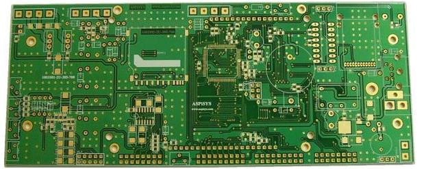
The composition of a PCB board is a multi-layer structure using a series of lamination, wiring and prepreg processing on the vertical stack. In the multi-layer PCB board, in order to facilitate debugging, the signal line will be laid on the outermost layer.
In the case of high frequency, the distributed inductance and distributed capacitance of the PCB board, such as traces, vias, resistors, capacitors, and connectors, cannot be ignored. Resistance will cause reflection and absorption of high-frequency signals. The distributed capacitance of the trace will also play a role. When the length of the trace is greater than 1/20 of the corresponding wavelength of the noise frequency, an antenna effect occurs, and noise is emitted through the trace.
Most of the wire connections of the PCB board are completed through vias. One via can bring about 0.5pF distributed capacitance, and reducing the number of vias can significantly increase the speed.
The packaging material of an integrated circuit itself introduces a capacitance of 2 to 6 pF. A connector on the PCB has a distributed inductance of 520nH. A dual-in-line 24-pin integrated circuit socket introduces 4-18nH distributed inductance.