1. The 4-layer board from top to bottom is: signal plane layer, ground, power supply, signal plane layer;
The 6-layer board from top to bottom is: signal plane layer, ground, signal inner electric layer, signal inner electric layer, power supply, signal plane layer. For boards with 6 or more layers (the advantage is: anti-interference radiation), the inner electric layer is preferentially routed, and the inner electric layer cannot meet the design requirements, then the plane layer is selected for wiring. It is forbidden to route wires from the ground plane or power plane (reason: it will divide the power plane and produce parasitic effects).
2. If FPGA devices are required in the designed PCB, the Quartus II software must be used to verify the pin assignments before drawing the schematic. (Some special pins in FPGA cannot be used as ordinary IO).
3. Wiring of multi-power supply system:
If the FPGA+DSP system is used as a 6-layer board, there will usually be at least 3.3V+1.2V+1.8V+5V.
3.3V is generally the main power supply, and the power layer is directly laid, and the global power supply network can be easily routed through the vias;
5V may generally be the power input, and only a small area of copper is required. And as thick as possible.

1.2V and 1.8V are the core power supply (if you directly use the wire connection method, you will encounter great difficulties when facing BGA devices). Try to separate 1.2V and 1.8V during layout, and let 1.2V or 1.8V connect The components are arranged in a compact area and connected by copper skin.
In short, because the power supply network is spread over the entire PCB, it will be very complicated and long to go around if it is routed. The method of laying copper is a good choice!
4. The wiring between the adjacent layers of the multilayer board adopts a cross method, the purpose is: to reduce the electromagnetic interference between the parallel wires, and to facilitate the wiring.
5. The analog circuit and the digital circuit should be isolated. How to use the isolation method? Separate the devices used for analog signals from the devices of digital signals during layout, and then cut across the AD chip! The analog signal is laid with analog ground, analog ground/analog power supply and The digital power supply is connected at a single point through an inductor/magnetic bead.
6. PCB design based on PCB design software can also be regarded as a software development process. Software engineering pays most attention to the idea of "iterative development" to reduce the probability of PCB errors.
(1) Check the schematic diagram, pay special attention to the power and ground of the device (power and ground are the blood of the system, and there can be no negligence);
(2) PCB package drawing(confirm whether the pins in the schematic diagram are wrong);
(3) After confirming the PCB package size one by one, add a verification label and add it to the package library of this design;
(4) Import the netlist and adjust the signal sequence in the schematic while layout (OrCAD component automatic numbering function can no longer be used after layout);
(5) Manual wiring (check the power ground network while cloth, as I said before: the power network uses the copper method, so use less wiring);
In a word, the guiding ideology in PCB design is to draw back and correct the schematic diagram of the package layout while drawing (considering the correctness of signal connection and the convenience of signal routing).
7. The crystal oscillator should be as close as possible to the chip, and there should be no wiring under the crystal oscillator, and the network copper skin should be laid. Clocks used in many places are wired in a tree-shaped clock tree.
8. The arrangement of the signals on the connector has a great influence on the difficulty of wiring, so it is necessary to adjust the signals on the schematic while wiring (but do not renumber the components).
9. Design of multi-board connector:
(1) Use flat cable connection: the upper and lower interfaces are the same;
(2) Straight socket: the upper and lower interfaces are mirrored and symmetrical,
10. Design of module connection signal:
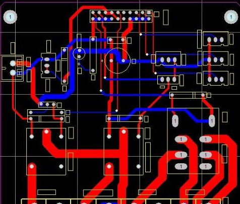
(1) If the two modules are placed on the same side of the PCB, then the serial number of the supervisor should connect to the small and connect to the large (mirror connection signal);
(2) If two modules are placed on different sides of the PCB, then the serial number of the control system should be connected to small and large.
Doing so will place the signal to cross as in the right picture above. Of course, the above method is not a rule. I always say that everything changes as needed (this can only be understood by yourself), but in many cases, designing in this way is very useful.
11. Design of power ground loop:
The ground loop area of the power supply is large, and it is susceptible to electromagnetic interference. Through the improvement-the power supply and the ground wire are close to the wiring, which reduces the loop area and reduces the electromagnetic interference (679/12.8, about 54 times). Therefore, the power and ground should be as close as possible to the trace! And the signal line should be avoided as much as possible to run the line to reduce the mutual inductance effect between the signals.
12. Choose a good grounding point: the grounding point is often the most important
I don’t know how many engineers and technicians have talked about the small grounding point, which shows its importance. Under normal circumstances, a common ground is required, such as: multiple ground wires of the forward amplifier should be merged and then connected to the main ground, and so on. In reality, it is difficult to achieve this completely due to various restrictions, but we should try our best to follow it. This problem is quite flexible in practice. Everyone has their own set of solutions. It is easy to understand if they can explain it for a specific circuit board.
13. There must be a reasonable direction
Such as input/output, AC/DC, strong/weak signal, high frequency/low frequency, high voltage/low voltage, etc. Their direction should be linear (or separated), and they should not blend with each other. Its purpose is to prevent mutual interference. The best trend is in a straight line, but it is generally not easy to achieve. The most unfavorable trend is a circle. Fortunately, isolation can be set to improve. For DC, small signal, low voltage PCB design requirements can be lower. So "reasonable" is relative.
14. Reasonably arrange power filter/decoupling capacitors
Generally, only a number of power filter/decoupling capacitors are drawn in the schematic, but they are not pointed out where they should be connected. In fact, these capacitors are set up for switching devices (gate circuits) or other components that require filtering/decoupling. These capacitors should be placed as close as possible to these components. If they are too far away, they will have no effect. Interestingly, when the power supply filter/decoupling capacitors are arranged properly, the problem of the grounding point becomes less obvious.
15. The wire diameter of the line requires the size of the buried hole to be appropriate
If possible, wide lines should never be thin; high-voltage and high-frequency lines should be round and slippery, without sharp chamfers, and corners should not be at right angles. The ground wire should be as wide as possible, and it is best to use a large area of copper, which can greatly improve the problem of grounding points. The size of the pad or via is too small, or the size of the pad and the hole size are not properly matched. The former is unfavorable for manual drilling, and the latter is unfavorable for CNC drilling. It is easy to drill the pads into a "c" shape, and to drill off the pads. The wire is too thin, and the large area of the unwiring area is not provided with copper, which is easy to cause uneven corrosion. That is, when the unwiring area is corroded, the thin wire is likely to be over corroded, or it may appear to be broken, or completely broken. Therefore, the role of setting copper is not only to increase the area of the ground wire and anti-interference.
16. Number of vias, solder joints and line density
Some problems are not easy to be found in the early stage of circuit production, and they tend to emerge in the later stage. For example, if there are too many wire holes, the slightest carelessness in the copper sinking process will bury hidden dangers. Therefore, the design should minimize the line holes. The density of parallel lines in the same direction is too large, and it is easy to join together when welding. Therefore, the line density should be determined according to the level of the welding process. The distance of the solder joints is too small, which is not conducive to manual welding, and the welding quality can only be solved by reducing the work efficiency. Otherwise, hidden dangers will remain. Therefore, the minimum distance of solder joints should be determined by comprehensive consideration of the quality and work efficiency of the welding personnel.
If you can fully understand and master the above-mentioned PCB circuit board design precautions, the PCB factory can greatly improve the design efficiency and product quality. Correcting the existing errors during production will save a lot of time and cost, and save rework time and material input.