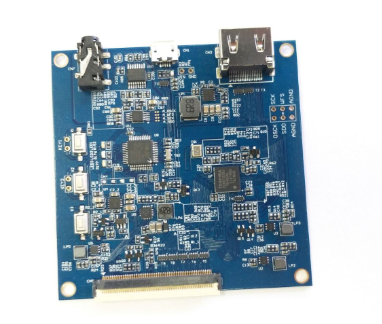
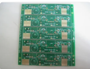
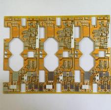
The basic composition of PCBs seen in daily life is generally solder mask, silk screen layer, copper wire, etc. In other words, we call the part of the PCB surface printed with green paint as the solder mask; and the solder mask uses negative output during the production process, so after the shape of the solder mask is mapped to the PCB, it is not applied. The green oil solder mask, on the contrary, exposed the copper skin. The role of the solder mask in controlling the reflow soldering process is very important.
The solar solder mask process in PCB printing production is a printed board with solder mask after screen printing. Cover the pads on the printed board with an exposure master so that it will not be irradiated by ultraviolet light during exposure, while the solder resist protection layer is more firmly attached to the printed board surface after ultraviolet light irradiation, and the pads are not exposed to ultraviolet light Irradiation can expose the copper pads so that lead and tin can be applied during hot air leveling. Today, Lao Chen wants to focus on the process of solder mask.
1. Pre-bake
Pre-bake is to evaporate the solvent contained in the ink to make the solder resist film into a non-stick state. The type of ink is different, the temperature and time of its pre-bake are also different. If the drying time is too long, or the pre-bake temperature is too high, it will reduce the resolution and cause poor development; if the pre-bake time is too short or the temperature is too low, the film will stick during exposure, and the solder mask will be exposed to sodium carbonate solution during development. Corrosion, causing the surface to lose luster or the solder mask to swell and fall off.

2. Exposure
Exposure is the key to the entire process. If overexposure, due to the scattering of light, the solder resist film on the edge of the pattern or line reacts with light (mainly the photosensitive polymer contained in the solder resist reacts with light), resulting in a residual film, which reduces the resolution and causes the development of the film. The pattern becomes smaller and the lines become thinner; if the exposure is under-exposed, the result is contrary to the above situation, the developed pattern becomes larger and the lines become thicker. This situation can be reflected by the test: if the exposure time is long, the measured line width is a negative tolerance; if the exposure time is short, the measured line width is a positive tolerance. In the actual process, a "light energy integrator" can be used to determine the best exposure time.
3. Ink viscosity adjustment
The viscosity of the dynamic photosensitive solder resist ink is mainly controlled by the ratio of the hardener to the main agent and the added amount of the diluent. If the amount of hardener added is not enough, an imbalance of ink characteristics may occur.
Looking back at the present, 2020 will be a year when the world's 5G communication development has exploded. In daily design and use, the low Dk/Df material performance of 5G communication is mainly determined by plates, followed by solder mask inks. But what we cannot ignore is that the domestic PCB ink production and manufacturing, especially the IC package substrate solder mask ink, automotive electronics PCB solder mask oil, solder mask dry film, and other technologies still have a large gap with the world's advanced level. In the final process of the solder mask-paint spraying, the way we use:
The spraying technology of solder mask ink currently has more mature applications including screen printing, electrostatic spraying, low-pressure spraying and other technologies. The following Lao Chen will show you the advantages and disadvantages of these methods. Screen printing requires a large number of skilled screen printing personnel (note that the quality and experience of the screen printing personnel must be ensured here). It is precisely because of the greatest demand for manpower that this is generally the most ink-saving coating method. For the same screen printing, if an automatic screen printing machine is used, it is more suitable for large-volume boards; but expensive is not his shortcoming, but my shortcoming; in addition, this kind of mass-produced machine is very insensitive to small-batch PCBs. friendly. Electrostatic spraying technology is very mature and can save a lot of labor. Both prototypes and batch boards are applicable, but the ink consumption is large, the equipment is relatively expensive, and the maintenance cost is high; low-pressure spraying technology still needs to be optimized and improved in many places, and the ink consumption is large., But the advantage is that the equipment is relatively cheap and the maintenance cost is low. It remains to be seen whether low-pressure spraying technology can become the mainstream coating technology, and the number of people currently used is small.
Ink-jet printing solder mask inks are relatively a gradual development process. The research results of a large number of PCB companies in the past few years show that a considerable number of companies have not continued to develop new inkjet processes. Current applications depend on the development of ink raw materials and equipment. Moreover, there are very few types of materials available for inkjet printing and solder resist inks, and the accuracy and efficiency of the equipment need to be improved. These are the shortcomings of the current inkjet printing solder mask, and they are also the direction we are working hard for.