How to deal with the problems of "via hole cover oil" and "via hole opening window" in PCB processing?
Regarding the point of "Via window opening" and "Via hole cover oil" (the usage distinction between PAD and VIA), many customers and PCB design engineers often ask what this means when placing an order. Which option should be selected for the file?
Now the description of this problem is as follows:
I often encounter such problems. The PCB design is seriously non-standard. It is impossible to distinguish between the pad and the usage of via. Sometimes the conductive hole is processed by the attribute of the pad, and sometimes the plug-in hole is processed by the attribute of the via. VIA The design of attributes and PAD attributes is confused, leading to incorrect processing. This is also one of the problems that often complains. For circuit board production plants, when processing CAM data, some processing film engineers will make mistakes because the customer’s design documents are not standardized. Help customers modify documents, correct irregular designs, and process engineering data based on their own experience, which has led to and contributed to the irregular designs of customers.

The PCB processing factory hereby clarifies: the last time you did the right thing, it does not mean that the file is right! All engineers must pay attention to design standards and specifications! The PCB processing factory will again strictly require all processing engineers to maintain the status quo of customer documents as much as possible! Try to deal with the design specifications and standards as much as possible, not according to the so-called experience! Reflect the problem, this can be a reference for PCB design engineers, improve the design quality and reduce the occurrence of problems!
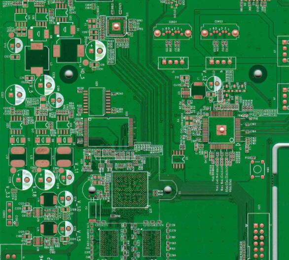
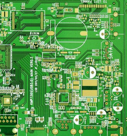
This article mainly explains the connection between conductive holes, plug-in holes, and protel /pads/ and geber files. Conductive holes: via, plug-in holes: pads are particularly prone to problems:
1. During the via conversion process, due to non-standard design or unclear settings of the conversion gerber rules, the problem is that the gerber file is the only one that can be identified by the factory manufacturer. Those are via holes and those are plug-in holes. It is processed according to the file, and there is a window if there is a soldering layer!
2. The pad and via are mixed together, causing problems
1. When the file is pads or protel, send it to the factory. It requires via hole cover oil. Please pay attention to carefully check whether the plug-in hole (pad) is also available via via, otherwise the plug-in hole will also be up. The green oil prevents welding.
2. When the file is protel or pads, send the file to the PCB factory. The order requirement is via hole cover oil. Many customers use pads (plug-in holes) to indicate conductive holes, which causes the conductive holes to open windows, which may be via holes. Cover oil, the point of contention at that time is that what you want is conductive hole cover oil, why the window is opened, then please check the file design!
The PCB processing factory will explain this point again as follows, if it is via, it will be processed by via, if it is a pad, it will be processed by pad! Because no one will know which is the conductive hole, which is the plug-in hole, and via and pad are the only signs, please be clear!
3. How to design via hole cover oil in protel or pads! --This is the most standard way. If the design is standard, there will be no mistakes!
There is a tenting option in the via attribute in Protel. If you check it, it must be covered with oil. Then all the transferred files are covered with oil. In pads, when you transfer files from pads, you need to think about the method of covering oil through holes (via): When outputting the soldermask, that is, the solder mask, just check the solder mask top-the via below represents all vias and open windows. If you don't check it, the vias are covered with oil.