Everyone knows that to make a PCB board is to turn a designed schematic diagram into a real PCB circuit board. Please don't underestimate this process. There are many things that work in principle but are difficult to achieve in engineering, or What others can achieve, others can't. Therefore, it is not difficult to make a PCB board, but it is not easy to do a good PCB board.
The two major difficulties in the field of microelectronics are the processing of high-frequency signals and weak signals. In this regard, the level of PCB production is particularly important. The same principle design, the same components, and PCBs produced by different people have different results., Then how can we make a good PCB board? Based on our past experience, I would like to talk about my views on the following aspects:
1. Make clear design goals
Receiving a design task, we must first clarify its design goals, whether it is an ordinary PCB board, a high-frequency PCB board, a small signal processing PCB board, or a PCB board with both high frequency and small signal processing. If it is an ordinary PCB board, As long as the layout and wiring are reasonable and tidy, and the mechanical dimensions are accurate, if there are medium load lines and long lines, certain measures must be used to reduce the load, and the long line must be strengthened to drive, and the focus is to prevent long line reflections. When there are signal lines exceeding 40MHz on the board, special considerations should be made to these signal lines, such as crosstalk between lines. If the frequency is higher, there is a stricter limit on the length of the wiring. According to the network theory of distributed parameters, the interaction between the high-speed circuit and its wiring is a decisive factor and cannot be ignored in system design. As the gate transmission speed increases, the opposition on the signal lines will increase accordingly, and the crosstalk between adjacent signal lines will increase proportionally. Generally, the power consumption and heat dissipation of high-speed circuits are also very large, so high-speed PCBs are being made. Enough attention should be paid.
When there are millivolt or even microvolt-level weak signals on the board, these signal lines need special attention. Small signals are too weak and are very susceptible to interference from other strong signals. Shielding measures are often necessary, otherwise they will Greatly reduce the signal-to-noise ratio. As a result, the useful signal is submerged by noise and cannot be extracted effectively.
The commissioning of the board should also be considered in the design stage. The physical location of the test point, the isolation of the test point and other factors cannot be ignored, because some small signals and high-frequency signals cannot be directly added to the probe for measurement.
In addition, other relevant factors should be considered, such as the number of layers of the board, the package shape of the components used, and the mechanical strength of the board. Before making a PCB board, you must have a good idea of the design goals for the design.
2, understand the requirements of the layout and routing of the functions of the components used
We know that some special components have special requirements in the layout and routing, such as the analog signal amplifier used by LOTI and APH. The analog signal amplifier requires a stable power supply and small ripple. Keep the analog small signal part as far away from the power device as possible. On the OTI board, the small signal amplifying part is also specially equipped with a shielding cover to shield the stray electromagnetic interference. The GLINK chip used on the NTOI board uses ECL technology, which consumes a lot of power and generates heat. Special consideration must be given to the heat dissipation problem in the layout. If natural heat dissipation is used, the GLINK chip must be placed in a place with relatively smooth air circulation., And the heat radiated can not have a big impact on other chips. If the board is equipped with speakers or other high-power devices, it may cause serious pollution to the power supply. This point should also be paid enough attention.

3, the consideration of component layout
The first factor that must be considered in the layout of components is electrical performance. Put closely connected components together as much as possible, especially for some high-speed lines, make them as short as possible when laying out power signals and small signal devices. To be separated. On the premise of meeting the circuit performance, the components must be placed neatly and beautifully, and easy to test. The mechanical size of the board and the location of the socket must also be carefully considered.
The grounding and the transmission delay time on the interconnection line in the high-speed system are also the first factors to be considered in the system design. The transmission time on the signal line has a great influence on the overall system speed, especially for high-speed ECL circuits. Although the integrated circuit block itself is very fast, it is due to the use of ordinary interconnect lines on the backplane (the length of each 30cm line is about The delay amount of 2ns) increases the delay time, which can greatly reduce the system speed. Like shift registers, synchronous counters and other synchronous working components are best placed on the same plug-in board, because the transmission delay time of the clock signals to different plug-in boards is not equal, which may cause the shift register to produce major errors. On one board, where synchronization is the key, the length of the clock lines connected from the common clock source to the plug-in boards must be equal.
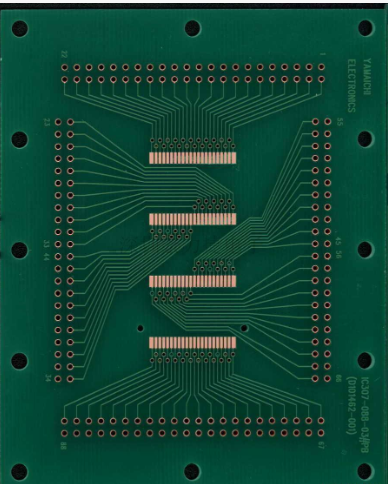
4, the wiring technology of the PCB board
Whether to choose a double-sided board or a multi-layer board when making a PCB depends on the highest operating frequency, the complexity of the circuit system, and the requirements for assembly density. It is best to choose a multilayer board when the clock frequency exceeds 200MHZ. If the operating frequency exceeds 350MHz, it is best to choose a printed circuit board with PTFE as the dielectric layer, because its high-frequency attenuation is smaller, the parasitic capacitance is smaller, and the transmission speed is faster. Large and low power consumption, the following principles are required for the wiring of the printed circuit board
(1) Keep as much space as possible between all parallel signal lines to reduce crosstalk. If there are two signal wires that are close together, it is best to run a ground wire between the two wires, which can play a shielding role.
(2) When designing signal transmission lines, avoid sharp turns to prevent reflections caused by sudden changes in the characteristic impedance of the transmission line. Try to design a uniform arc line with a certain size.
The width of the printed line can be calculated according to the above-mentioned characteristic impedance calculation formula of the microstrip line and the strip line. The characteristic impedance of the microstrip line on the printed circuit board is generally between 50 and 120Ω. To get a large characteristic impedance, the line width must be very narrow. But very thin lines are not easy to make. Considering various factors, it is generally appropriate to choose an impedance value of about 68Ω, because the characteristic impedance of 68Ω can achieve the best balance between delay time and power consumption. A 50Ω transmission line will consume more power; of course, a larger impedance can reduce the power consumption, but it will increase the transmission delay time. The negative line capacitance will increase the transmission delay time and decrease the characteristic impedance. However, the intrinsic capacitance per unit length of the line segment with very low characteristic impedance is relatively large, so the transmission delay time and characteristic impedance are less affected by the load capacitance. An important feature of a properly terminated transmission line is that the short branch line should have no effect on the line delay time. When Z0 is 50Ω. The length of the branch stub must be limited to 2.5 cm or less. In order to avoid loud ringing.
(4) For double-sided boards (or four-layer lines in six-layer boards). The lines on both sides of the circuit board should be perpendicular to each other to prevent crosstalk caused by mutual induction.
(5) If there are high-current devices on the printed circuit board, such as relays, indicator lights, speakers, etc., their ground wires should be separated to reduce noise on the ground wire. The ground wires of these high-current devices should Connect to an independent ground bus on the plug-in board and backplane, and these independent ground wires should also be connected to the ground point of the entire system.
(6) If there is a small signal amplifier on the board, the weak signal line before amplification should be far away from the strong signal line, and the trace should be as short as possible, and if possible, shield it with a ground wire.