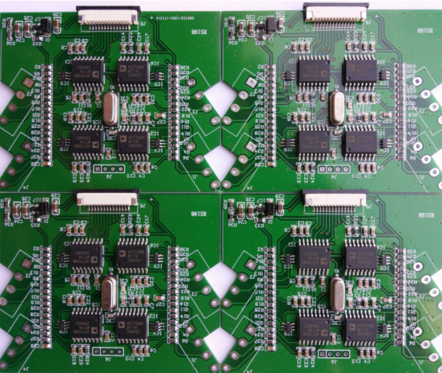
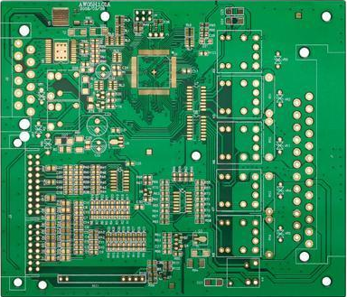
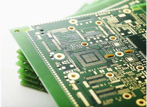
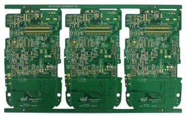
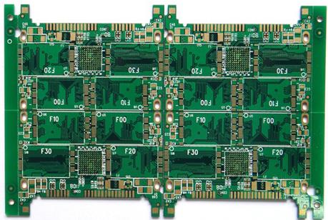
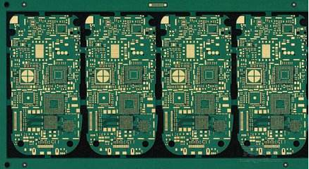
The printed circuit boards of the circuit board factory are mainly composed of insulating substrates, printed wires and pads.
Insulating substrate
Generally divided into organic substrate materials and inorganic substrate materials.
Organic substrate materials refer to reinforced materials such as glass fiber, impregnated with resin binder, dried into blanks, then covered with copper foil, and made by high temperature and high pressure. Such substrates are called copper clad laminates ( CCL), referred to as copper clad laminate, is the main material for manufacturing PCB.
Inorganic substrate materials are mainly ceramic plates and enamel-coated steel substrates. The material of the ceramic substrate is 96% alumina. The ceramic substrate is mainly used in hybrid integrated circuits and multi-chip micro-assembly circuits. It has the characteristics of high temperature resistance, smooth surface and high chemical stability. The enamel coated steel substrate overcomes the ceramic substrate The existing shortcomings of limited dimensions and high dielectric constant can be used as substrates for high-speed circuits and used in some digital products.
Printed wire
Generally, the printed wires are as wide as possible, which is good for withstanding current and easy for manufacturing. When determining the width of the printed wires, in addition to the current carrying capacity, attention should be paid to the peel strength of the copper foil on the board. The width of printed wires is recommended to adopt specifications of 0.5mm, 1.0mm, 1.5mm, 2.0mm. Among them, the current carrying capacity of the power cord and the grounding wire is relatively large. The overall design principle of the wire width is signal wire 
When the printed wire is designed to be connected to the SMT pad, it is generally not allowed to be directly connected between the relative gaps of the two pads. It is recommended to lead out at both ends before connecting; in order to prevent the integrated circuit from deflection during reflow soldering, solder with the integrated circuit In principle, the wires connected to the pad are led out from either end of the pad, but the surface tension of the pad should not be excessively concentrated on one side, and the solder tension on each side of the device should be balanced to ensure that the device will not occur relative to the pad. Deflection: When the width of the printed wire is large and needs to be connected to the component pad, it is generally necessary to narrow the wide wire to 0.25mm before connecting, and the length is not shorter than 0.65mm, and then connect to the pad. This avoids false welding.
Quality inspection of printed circuit boards
1. Visual inspection
Visual inspection refers to the manual inspection of printed circuit board defects. The inspection content includes surface finish, whether the silk screen is clear, whether the pad is round and whether the solder void is in the center of the pad. The method is to cover the processed negative with a photographic base map. On the printed circuit board, determine whether the edge size, wire width and shape of the printed circuit board are within the required range.
2. Electrical performance inspection
The electrical performance test mainly includes the insulation and connectivity of the circuit board. The insulation test mainly measures the insulation resistance. The insulation resistance can be carried out between the wires on the same layer or between different layers. Choose two or more closely spaced wires, measure the insulation resistance first, then humidify and heat for a certain period of time and return to room temperature before measuring again. The measurement of connectivity by the optical board tester is mainly to see whether the two points of the connection are connected according to the electrical schematic diagram.
3. Solderability inspection of pad
Pad solderability is an important indicator of PCB printed circuit boards. It mainly measures the wetting ability of solder on the printed pad, which is divided into three indicators: wetting, semi-wetting and non-wetting. Wetting means that the solder can flow and expand freely on the pad to form an adhesive connection. Semi-wetting means that the solder wets the surface of the pad first, and the solder shrinks due to poor wettability, resulting in a thin layer of solder on the base metal. Non-wetting means that although the solder is deposited on the pad, it does not form an adhesive connection with the pad.
4. Copper foil adhesion inspection
Copper foil adhesion refers to the adhesion of PCB printed wires and pads on the substrate. The adhesion is small, and the printed wires and pads are easy to peel from the substrate. To check the adhesion of the copper foil, you can use tape, stick the transparent tape on the wire to be tested, remove the air bubbles, and then quickly pull off the tape at a 90° direction to the printed circuit board. If the wire is intact, it means that the printed circuit board is The adhesion of copper foil is qualified.