In recent years, with the rapid development of new technology and devices, high-speed devices have become more and more popular, and high-speed circuit design has become a commonly needed technology. TI's DsPs chip TMS320C62xx, C64xx, C67xx series devices are one of the fast-growing high-speed devices. The C6000 internal structure is fixed-point, floating-point series compatible with DsP, the current CPU main frequency is 100MHz, -4i00MHz. With VelociTITM's advanced Very Long Instruction Word (VLIW) architecture core, it is possible to execute 8 32 bit instructions in one instruction cycle in parallel. Because of its high-speed computing ability, it is widely used in communication, electronic countermeasure, radar, image processing and other areas that require high intelligence and high-speed processing capabilities.
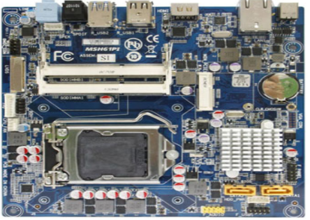
With the increasing degree of chip integration, more and more pins of the chip are added, and the packaging of devices is changing constantly, from DIP to OSOP, from SOP to PQFP, from PQFP to BGA. TMS320C6000 series devices are encapsulated by BGA. In circuit application, BGA encapsulation has the characteristics of high success rate, low repairing rate and high reliability, and is used more and more widely. However, because BGA encapsulation belongs to spherical raster array patch encapsulation, the physical implementation of the system in development, that is, board-level design involves many high-speed digital circuit design techniques. Noise interference is a major factor in high-speed systems. Radiation and conflicts occur in high-frequency circuits, while ringing, reflection and crosstalk occur at faster edge rates. If the particularity of high-speed signal layout and wiring is not considered, the designed circuit board will not work properly. Therefore, the success of PCB board design is a very critical part in the process of DSPs circuit design.

1 Transmission line effect
1.1 Signal Integrity
Signal integrity mainly includes reflection, ringing, ground bounce and crosstalk. The lines on the PCB board can be equivalent to the series and parallel capacitance, resistance and inductance structures shown in Fig. 1. Typical value of series resistance is 0.25D. /R-4). 55DJft, the shunt resistance value is usually very high. When parasitic resistance, capacitance, and inductance are added to an actual PCB connection, the final impedance on the connection is called the characteristic impedance zo.
If the impedance of the transmission line does not match that of the receiving end, this will cause reflection and oscillation of the signal.
PCB Routing Equivalent Circuit
The geometry of the wiring, the incorrect end connections, the transmission through the connector, and the discontinuity of the power plane all cause reflection. Over-shocks and down-shocks are generated when the signal changes along the rise and fall of the level. They can produce burrs above or below the steady level in an instant, which can easily damage the device. The ringing and surrounding oscillations of the signal are due to inappropriate inductance and capacitance on the line, respectively. Ring can be reduced by proper termination.
When there is a large current surge in the circuit, it will cause ground bounce. If there is a large transient current flowing through the power plane of the chip and the board, the parasitic inductance and resistance between the chip package and the power plane will cause power noise. Crosstalk is a coupling problem between two signal lines. The mutual inductance and mutual tolerance between signal lines cause noise on the lines. Capacitive coupling leads to coupling current, while inductive coupling leads to coupling voltage. The parameters of the PCB layer, the spacing between signal lines, the electrical characteristics of the driver and the receiver, and the way the lines are connected all have certain effects on the crosstalk.
1.2 Solutions
Some measures are needed to solve common problems:
The power layer has no restrictions on the direction of the current, and the return line can follow a path of impedance that is close to the signal line. This may result in a current loop, which will be the method for high-speed systems. However, the power layer does not eliminate line clutter and does not pay attention to the power distribution path, all systems will produce noise and cause errors. Therefore, special filters are needed, which are implemented by bypass capacitors. Generally, a capacitance from lshrimp to lOp.F is placed at the power input end of the board, while the capacitance from 0.01p.F to U0.1 center is placed between the power supply of each active device on the board and the pins of the ground. Bypass capacitance acts like a filter, where a large capacitance (10aF) is placed at the power input, low frequency (60Hz) noise is generated outside the board, and the noise generated by active devices on the board is harmonic at 100MHz or higher. The bypass capacitance placed between each chip is usually much smaller than that placed at the power input on the board.
As a rule of thumb, if you mix analog and digital in your design, divide the PCB into analog and digital parts, analog devices into analog parts, digital devices into digital parts, and A/D converters across regions. The analog and digital signals are wired in their respective areas to ensure that the return current of the digital signal does not flow to the ground of the analog signal.
Bypass and decoupling prevent energy from being transferred from one loop to another. Three loop areas, power layer, bottom layer, components and internal power connection, need to be considered. Widening the power supply and ground wire width as much as possible means that the ground wire is wider than the power cord. The relationship between them is: ground wire > power cord > signal line. Usually the signal line width is O.2-O.3mm, the thin width can be 0.05 "-'0.07mm, the power line is 1.2" -'2.5 n'Lrfl. Use a large area of copper as ground wire. Connect unused places to the ground on the printed board as ground wire. Or it can be made into a multilayer board, with one floor for the power supply and one floor for the ground wire. Configure a 0.01-center ceramic capacitor for each integrated circuit chip. If the space of printed circuit board is small and cannot be installed, a tantalum electrolytic capacitor can be configured with 1-10 chips every 4-10 chips. The high frequency impedance of this device is very small, the impedance is less than lQ in the range of 500 kI-Iz-20MHz, and the leakage current is very small (below O.5LlA). Decoupling filter capacitors must be installed close to integrated circuits in order to shorten capacitor leads and transient current circuit area, especially high frequency bypass capacitors.
When the system is working at 50MHz, transmission line effects and signal integrity problems will occur, and the traditional measures can achieve satisfactory results. When the system clock reaches 120MHz, it is necessary to consider the use of high-speed circuit design knowledge, otherwise PCB designed based on traditional methods will not work properly. Therefore, high-speed PCB circuit design has become a design technology that electronic system designers must master.
2 PCB High Speed Signal Circuit Design Technology
2.1 High speed signal wiring
Multilayer board is necessary for high-speed signal wiring as well as an effective means to reduce interference. To reduce the size of the printed circuit board, make full use of the middle layer to set shield, achieve close grounding, effectively reduce parasitic inductance, shorten the length of signal transmission, reduce cross-interference between signals and so on, all of which are beneficial to the reliability of high-speed circuits. Data show that the noise level of the four-layer panel is 20 dB lower than that of the two-panel panel panel when the same materials are collected in the 8th National Academic Symposium on Radiation-Resistant Electronics and Electromagnetic Pulse. The fewer bends in the lead, the better. Using a full straight line, a transition is required. A 45-degree polyline or arc transition can be used to reduce the external transmission and coupling of high-speed signals, and reduce the radiation and reflection of signals.
The shorter the lead between pins of high-speed circuit devices, the better. The longer the lead length, the greater the distributed inductance and capacitance value, which will lead to reflection, oscillation and so on in high-speed circuit system. The fewer alternations between lead layers between pins of high-speed circuit devices, the better, that is, the fewer holes are used in the process of component connection. It is estimated that a through hole can bring about a distributed capacitance of about 0.5pF, resulting in a significant increase in the delay of the circuit. In high-speed circuit wiring, attention should be paid to the "cross interference" introduced by the near parallel routes of the signal lines. If parallel distribution cannot be avoided, a large area of "ground" can be placed on the back of the parallel signal lines to reduce the interference. In the two adjacent layers, the direction of the line must be perpendicular to each other.
Enforce ground-line enclosure for particularly important signal lines or local units. Protected baselines can be added to the periphery while such non-interferable signals as clock signals, high-speed analog signals, etc. are traveling, and the signal cables to be protected are clamped in the middle. All kinds of signal routes cannot form loops, and ground wires cannot form current loops. If a loop wiring circuit is generated, it will cause a lot of interference in the system. The use of chrysanthemum* chain wiring can effectively avoid loops when wiring. One or more high frequency decoupling capacitors should be set near each IC block. High frequency choke is used when analog and digital ground lines connect to public ground lines. Some high-speed signal lines should be handled specially: differential signals require that they be on the same layer and as close as possible to parallel lines, and no signal is allowed to be inserted between the differential signal lines, and equal length is required.
High-speed signal wiring should avoid branching or stump formation as much as possible. High-frequency signal lines are prone to produce large electromagnetic radiation when walking on the surface. By wiring the high-frequency signal lines between the power supply and the wire, and absorbing the electromagnetic wave through the power supply and the bottom layer, the radiation generated will be much reduced.
2.2 High Speed Clock Signal Wiring
Clock circuit plays an important role in digital circuit. C64xDSP is a member of the C6000 platform and has a high processing speed. The high-speed clock of C64xDSP can reach 1.1GHz, which is lO times higher than that of earlier C62xDSP. Therefore, the clock wiring requirements will become increasingly high in the future application design of modern electronic systems based on DSP. High-speed clock signal line priority, in general, when wiring, needs to give priority to the main clock signal line of the system. High-speed clock signal line has a high frequency, which requires that the line be as short as possible to ensure signal distortion.
High frequency clock, particularly sensitive to noise interference. High frequency clock signal lines need to be protected and shielded to reduce interference.
High-frequency clocks (clocks above 20MHz, or clocks rising along less than 5ns) must have a ground wire escort with a line width of at least 10rail and a ground wire width of at least 20mil. The protective ground wire ends of the high frequency signal line must be well contacted with the ground through the holes and connected with the ground every 5em or so. Ground wire escort and data line are basically the same length, manual wire pulling is recommended; The clock sending side must be connected with a damping resistance of about 22-220Q in series. High-speed clock signal routing is designed as far as possible on the same layer, and there are no other disturbing sources and routing around the high-speed clock signal line. Star connection or point-to-point connection is recommended for high frequency clock connection. T connection should ensure equal arm length, minimize excess Ls, and copper should be applied under crystal oscillator or clock chip to prevent interference. Avoid interference from signal noise caused by these lines.
In high-speed signal wiring and high-speed clock signal wiring, it is required that less LL and less branching be played during the wiring to avoid stump and signal reflection and crossing. The influence of through-hole and stump (Stub) in high-speed PCB is not only reflected in the influence on signal, but also in the change of conductor impedance. However, the influence of holes and stumps on impedance is often neglected by designers.
To select a reasonable size of the hole. For example, for PCB designs with layers 4 to 10, the common choices are 10mil/20mil (drilling/bonding pad) or 16mil/30mil. For some small PCBs with high density, 8mil/18mil holes can also be used. Consider using a larger size to reduce impedance for power or ground wire passes. Place the pins of the power supply and ground close to the holes. The shorter the lead between the pins and the holes, the better. At the same time, the pins of the power supply and the ground should be as thick as possible to reduce impedance.
High density system-level chips are encapsulated in BGA or COB, and the pin spacing decreases day by day. The ball spacing is as low as O.6mm and will continue to decrease, making it impossible for the signal wires of the encapsulator to be drawn using traditional wiring tools. There are currently two ways to solve this problem in the 8th National Academic Symposium on Radiation-Resistant Electronics and Electromagnetic Pulses (249): (1) Draw the signal line from the lower layer through the hole under the ball; (2) Find a lead channel in the spherical grid array by using very thin wiring and free angle wiring. For such BGA or COB packaged high density devices, wiring with a very small width and space is the only viable option. Only in this way can high yield and reliability be guaranteed and high speed design requirements be met.
Design of 2.3 BGA encapsulated bonding pad
With the development of device packaging technology, the relative size of device packaging is getting smaller and smaller. The TMS320C6000 series devices have up to 352 pins, because the BGA feet are closely spaced and the holes are close to the pins, which can produce a large inductance. It is also harmful to high-speed signals, so when BGA disperses, try to use smaller holes. There is a corresponding relationship between the size of the BGA pad and the foot spacing of the BGA, but it cannot be larger than the diameter of the BGA pin ball, usually about 1/10~l/5 of it. Holes next to the BGA pad and the pad on the surface of the components need to be plugged and covered with green oil. For BGA welding, no other components can appear in the surrounding 2era.
Conclusion
Digital signal processor is signal processing. With the popularity of high frequency devices, the density of printed circuit board increases, the interference increases, and the improvement of signal quality has been put on the top position of design. The PCB board design of high-speed DSPs is a very complex process. Several factors need to be considered in the design of high-speed circuits, which correspond to each other. If the high-speed devices are laid out close to each other, the delay may be reduced, but crosstalk and significant thermal effects may occur. It is also a contradiction that high-speed signals should be wired as far as possible in the inner layer and fewer holes should be punched. Therefore, in the design, we need to take into account all the favorable factors to make a comprehensive circuit design.
Only in this way can a high quality PCB circuit board with strong anti-jamming ability, stable performance and high real-time performance be designed.