Incoming inspection of SMT process
Because in the SMT process of the circuit board manufacturer, the solder paste printing, the operation of the placement machine, and the soldering of the reflow soldering furnace should be listed as key processes, so the description is first from the incoming inspection in the SMT processing.
Inspection before assembly (incoming inspection)
1. Inspection method
The inspection methods mainly include visual inspection, automatic optical inspection (AOI), X-ray inspection and ultrasonic inspection, on-line inspection, functional inspection, etc.
(1) Visual inspection refers to the method of inspecting the assembly quality directly with the naked eye or with the help of magnifying glass, microscope and other tools.
(2) Automatic optical inspection (AOI), mainly used for process inspection: solder paste printing quality inspection after printing machine, mounting quality inspection after mounting, and post-welding inspection after reflow soldering furnace. Automatic optical inspection is used for Alternative to visual inspection: X-ray inspection and ultrasonic inspection are mainly used for solder joint inspection of BGA, CSP and Flip Chip.
(3) On-line testing equipment adopts special isolation technology to test the resistance of resistors, capacitance of capacitors, inductance of inductors, polarity of devices, as well as short circuit (bridge), open circuit (open circuit) and other parameters, and automatically diagnose Errors and failures, and errors and failures can be displayed and printed out.

(4) Function test is used for electrical function test and inspection of surface mount board. Functional testing is to assemble a board or table on the surface. The unit under test on the surface assembly board inputs electrical signals as a functional body, and then detects the output signal according to the design requirements of the functional body. Most functional tests have diagnostic programs that can identify and determine faults. However, the price of functional testing equipment is relatively expensive. The simplest function test is to connect the surface mount board to the corresponding circuit of the device to power up to see if the device can operate normally. This method is simple and requires less investment, but it cannot automatically diagnose faults.
Which method is used should be determined according to the specific conditions of each unit's SMT production line and the assembly density of the surface mount board.
2. Incoming Material Inspection
Incoming inspection is the primary condition to ensure the quality of surface assembly. The quality of components, printed circuit boards, and surface assembly materials directly affect the assembly quality of surface assembly boards. Therefore, the electrical performance parameters of components and the solderability of soldering tips and pins; the productivity design of printed circuit boards and the solderability of pads; solder paste, patch glue, rod-shaped solder, flux, cleaning agent The quality of surface mounting materials must have a strict incoming inspection and management system.
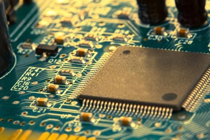
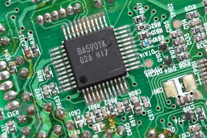
3. Inspection of surface mount components (SMC/SMD)
The main inspection items of components: solderability, pin coplanarity and usability should be sampled by the inspection department. The solderability of components can be tested by holding the component body with stainless steel tweezers and immersing it in a tin pot at 235 degree Celsius±5 degree Celsius or 230 degree Celsius±5 degree Celsius. Take it out at 2±0.2s or 3±0.5s, and inspect under a 20x microscope. Welding condition of soldering ends. 90% of soldering ends of components are required to be wetted with tin. As a processing workshop, the following visual inspections can be done:
(1) Visually or with a magnifying glass, check whether the solder ends or pin surfaces of the components are oxidized and whether there are contaminants.
(2) The nominal value, specification, model, accuracy, and external dimensions of the components should be consistent with the product process requirements. (3) The pins of SOT and SOIC should not be deformed. For multi-lead devices QFP with lead pitch less than 0.65mm, the pin coplanarity should be less than 0.1mm (optical inspection by the placement machine). (4) For products that require cleaning, the mark of the components will not fall off after cleaning, and will not affect the performance and reliability of the components (visual inspection after cleaning).
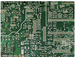
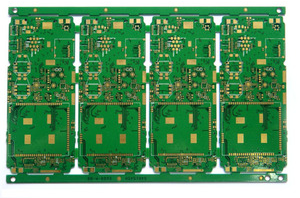
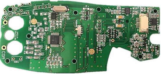
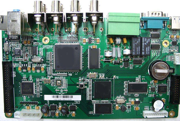
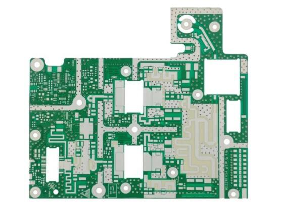
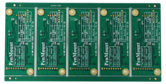
4. Printed circuit board(PCB) inspection
(1) PCB land pattern and size, solder mask, silk screen, and via hole settings should meet the design requirements of SMT printed circuit boards. (Example: Check whether the pad spacing is reasonable, whether the screen is printed on the pad, whether the via is made on the pad, etc.).
(2) The external dimensions of the PCB should be consistent, and the external dimensions, positioning holes, and reference marks of the PCB should meet the requirements of the production line equipment.
(3) PCB allowable warpage size:
1. Upward/convex surface: Maximum 0.2mm/5Omm and maximum length 0.5mm/the length of the whole PCB.
2. Downward/concave surface: maximum 0.2mm/5Omm, maximum length 1.5mm/the length of the whole PCB.
(4) Check whether the PCB is contaminated or damp