How to avoid poor PCB materials or deformation of SMT processing?
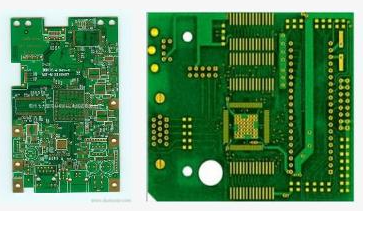
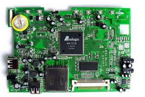
PCBA circuit board can be said to be the basis of electronic equipment. If the foundation is not flat, key components and semiconductors are not well-fitted, coupled with automated high-speed production, often lead to empty soldering of components or poor assembly status of components like tombstones. If the problem is small, the function of the electronic circuit is unstable, and if the problem is large, it may cause malfunction or short circuit/open circuit failure.
Automated production of PCB board flatness affects production yield
Especially in the production line environment of mass production, the new generation of electronic equipment production lines mostly use automatic SMT (surface-mount devices) feeding and automatic reflow component mechanisms, and the high-speed operation of the soldering/feeding from the soldering/feeding is carried out by automated equipment., It is no longer what manual processing can handle, even in a large number of miniature product structures, volumes, and the layout of components are more compact, most of which require automated production equipment to complete the processing procedures.

In the production process of automated processing equipment, the position and positioning calibration of automatic feeding is basically carried out when the PCB is fully flat. In order to obtain the production speed, the reciprocating feeding and positioning procedures may be accelerated or reduced due to the production speed. PCB board warping or deformation occurs during the production process or before processing and loading. The aforementioned problems may occur when large IC semiconductor loading or SMT component soldering and loading, resulting in a decrease in product quality and stability. The heavy processing of good products has caused the cost to skyrocket.
During the SMT processing and feeding process, the uneven PCB board will not only cause insufficient positioning of the feeding, but also large-scale power components may not be accurately inserted or mounted on the PCB surface. In poor conditions, the insertion machine may malfunction due to the wrong plug-in., The production speed of the automated production line drops due to the occurrence/removal of problems.
As for the components with skewed plug-ins, they may not affect the plug-in or welding production, but although the skewed components do not affect the function, they may cause problems in subsequent chassis assembly that cannot be installed in the chassis or assembly processing. Manual reprocessing afterwards will also cause heavy work. cost. In particular, SMT technology is being upgraded in the direction of high-speed, intelligent, and high-precision, but the easy warpage of PCB boards has often become a bottleneck that hinders further increases in production speed.
SMT automated processing, feeding accuracy is the focus of optimization
Take the SMT processing automation machine as an example. The components use the suction nozzle to suck the electronic components. The PCB is heated and the solder paste is quickly applied to the components to achieve a perfect loading/soldering state. It must be a component The suction is stable and the solder paste heat treatment time is just right. After the electronic components are completely connected with the PCB, the suction nozzle that sucks the material parts releases the vacuum suction and releases the material parts, completing the purpose of precise feeding/welding components.
During the loading process, the suction nozzle vacuum suction may be poorly controlled, causing component throwing problems, causing component displacement, or excessive pressure on the placement machine, causing the solder paste at the solder joints of the parts to be squeezed out of the solder joints. These conditions, especially when the PCB is warped and uneven, are most likely to be highlighted. The uneven PCB has also become a problem that the automatic feeder frequently needs to eliminate.
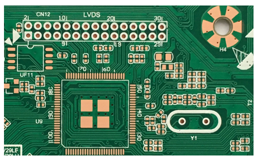
The unevenness of the PCB will not only cause throwing or extrusion of materials, but also for semiconductors and integrated chip components with dense pins. It is also very easy to shift from left to right (translation error) or angle (rotation error). The loading position is offset, and the result of the offset may cause the problem of soldering or even soldering of the semiconductor IC pins.
The lower the allowable PCB deformation, the better
The standards listed in the IPC mention that the maximum allowable deformation of the PCB corresponding to the SMT placement machine is about 0.75%. If the PCB does not enter the automatic SMT processing, manual loading/soldering, the maximum allowable deformation is 1.5%, but Basically, this is only a low standard requirement for the degree of PCB warpage. To meet the automatic processing accuracy and pre-determination of the SMT placement machine, the control standard for the PCB deformation must be higher than 0.75%, and it may be necessary to require at least 0.5 % Or even 0.3% high standard requirements.
Check why the PCB is warped? In fact, PCB is a composite board made of copper foil, glass fiber, resin and other composite materials using chemical rubber with physical pressing and bonding. Each material has different elasticity, expansion coefficient, hardness, and stress performance, and the condition of thermal expansion There will also be differences. In the PCB processing process, multiple heat treatments, mechanical cutting, chemical material soaking, physical pressure bonding and other processes are repeated. The production of a completely flat PCB is inherently difficult and difficult, but at least it can be controlled. Flatness performance required in a certain proportion.
The cause of PCB warpage is complicated and must be analyzed from various aspects of material/process
Although the cause of PCB warpage is complicated, it can be dealt with at least from a few angles that can be started. First of all, it is necessary to analyze the reason why the PCB board is deformed. Only when the key to the output problem is known can the corresponding solution be found. The problem of reducing the deformation of the PCB board can be thought and researched from the aspects of material, composite board structure, etching circuit pattern distribution, and processing process. .
Most of the causes of PCB warpage will occur in the PCB process itself, because when the copper area on the circuit board is different, for example, the circuit board will deliberately use a large area to improve electromagnetic problems or optimize electrical characteristics. Processing, and the data lines are relatively intensively etched, which will cause local area differences in the copper clad of the PCB itself, when a large area of copper clad copper foil cannot be evenly distributed on the same PCB.
When the heat generated by the operation of the equipment, or the heat generated by the processing machinery and processing, will cause the physical phenomenon of thermal expansion and contraction of the PCBA, and the uneven copper coating will cause local stress differences, the circuit board warpage will occur spontaneously, if the heat of the board The stress difference caused by expansion and contraction reaches the material limit value, which will cause permanent warpage and deformation of the PCB.