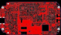
Analysis of high frequency circuit in CAD
When the operating frequency is higher (about 2GHz), the signal wavelength can gradually match the device size. The impedance of chip inductor shows obvious distribution characteristics, that is, different impedance exists in different reference positions. At high frequency, the circuit response of the device varies with its size and spatial structure. The conventional impedance measurement parameters can not accurately reflect the response characteristics of the actual circuit. Taking the RF power amplifier circuit of a mobile phone as an example, two high-frequency inductors (working frequency 1.9GHz) used for impedance matching are photolithographic thin-film inductors. If the laminated chip inductors (measuring instrument hp-4291b) with the same specifications and accuracy but significantly higher Q value are replaced, the transmission gain of the circuit will drop by nearly 10%. It shows that the matching state of the circuit is declining. It is obviously unable to accurately explain the application of high frequency by using the low frequency analysis method. It is not appropriate, at least not enough, to pay attention to the high frequency analysis of chip inductors with L and q.
Electromagnetic field theory is often used to analyze the high frequency application problems with distribution characteristics in engineering. Generally, in the measurement of chip inductor by impedance analyzer (hp-4291b), the measurement accuracy can be improved to about 0.1nh by means of fixture compensation and instrument calibration, which is sufficient to ensure the accuracy requirements of circuit design in theory. However, the problem that can not be ignored is that the measurement results at this time only reflect the parameter performance between the end electrode interfaces of the inductance device under the matching state (the measuring fixture is designed to accurately match), but the internal electromagnetic distribution and external electromagnetic environment requirements of the inductance device are not reflected. The inductors with the same test parameters may have completely different electromagnetic distribution due to different inner electrode structures. Under high frequency conditions, the actual circuit application environment (approximate matching, dense mounting, PCB distribution influence) of chip inductors is often different from the test environment. It is very easy to produce various complex near-field reflections, resulting in slight changes of actual response parameters (L, q). For the low inductance in RF circuit, this influence can not be ignored, we call it "distributed influence".
In the design of high-frequency circuit (including high-speed digital circuit), considering the circuit performance, device selection and electromagnetic compatibility, the working performance of the actual circuit system is generally considered by means of network scattering analysis (s parameter), signal integrity analysis, electromagnetic simulation analysis, circuit simulation analysis, etc. In view of the "distributed influence" problem of chip inductors, a feasible solution is to carry out structural electromagnetic simulation on the inductor and accurately extract the corresponding SPICE circuit model parameters as the basis of circuit design, so as to effectively reduce the error influence of inductance devices in high frequency design application. Most of the technical parameters of chip inductors produced by foreign (Japanese) main component enterprises contain s parameter, which can be used for accurate high frequency application analysis.