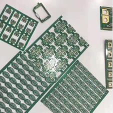
Analysis on the reasons and improvement methods of PCB open circuit
PCB circuit openings and short circuits are problems that PCB manufacturers encounter almost every day. They have been plagued by production and quality management personnel, resulting in insufficient shipments and replenishment, affecting on-time delivery, causing customer complaints, and it is more difficult for people in the industry. solved problem.
The reasons for the above phenomenon and the improvement methods are listed as follows:
1. Open circuit caused by exposed substrate
1. There are scratches before the copper clad laminate is put into the warehouse;
2. The copper clad laminate is scratched during the cutting process;
3. The copper clad laminate is scratched by the drill tip during drilling;
4. The copper clad laminate is scratched during the transfer process;
5. The copper foil on the surface was bumped due to improper operation when stacking the boards after copper sinking;
6. The copper foil on the surface of the production board is scratched when it passes through the leveling machine;
Improve methods:
1. IQC must conduct random inspections of copper clad laminates before entering the warehouse to check whether the surface of the board is scratched and exposed to the base material. If so, contact the supplier in time and make appropriate treatment according to the actual situation.

2. The copper clad laminate is scratched during the opening process. The main reason is that there are hard sharp objects on the table of the opener. The copper clad laminate and the sharp objects rub against the sharp objects during the opening process, which causes the copper foil to be scratched and form the phenomenon of exposed substrate. The table must be carefully cleaned before cutting to ensure that the table is smooth and free of hard and sharp objects.
3. Scratched due to improper operation after copper sinking and full plate electroplating: When storing boards after copper sinking or full plate electroplating, the weight is not light when the plates are stacked together and then put down., The board angle is downward and there is a gravitational acceleration, forming a strong impact force to hit the board surface, causing the board surface to scratch the exposed substrate.
4. The production board is scratched when it passes through the horizontal machine: the baffle of the grinder sometimes touches the surface of the board, and the edge of the baffle is uneven, which makes the utensils bulge, and the surface of the board is scratched when passing the board; stainless steel transmission The shaft is damaged into a sharp object, and the copper surface is scratched when passing the board, and the base material is exposed.
5. The PCB copper clad laminate was scratched by the drill nozzle during drilling. The main reason was that the spindle clamp nozzle was worn, or there were debris in the clamp nozzle that was not cleaned, and the drill nozzle could not be grasped firmly, and the drill nozzle did not reach the top. Slightly longer than the set length of the drill tip, the lifting height is not enough when drilling, and the tip of the drill tip scratches the copper foil when the machine tool moves, resulting in a phenomenon that the base material is exposed. The chuck can be replaced by the number of times recorded by the knife or according to the degree of wear of the chuck; the chuck should be cleaned regularly according to the operating rules to ensure that there is no debris in the chuck.
To sum up, for the phenomenon of scratching and exposing the substrate after copper sinking, it is easy to judge if the line is manifested in the form of open circuit or line gap; if it is the scratching and exposing substrate before copper sinking, it is easy to judge. When it is on the line, after the copper is sinked, a layer of copper is deposited, and the thickness of the copper foil of the line is obviously reduced. It is difficult to detect the open and short circuit test later, so that the customer may not be able to withstand it too much when using it. The circuit is burnt due to the high current, the potential quality problems and the resulting economic losses are quite large.
Two, non-porous opening
1. Immersion copper is non-porous;
2. There is oil in the hole to make it non-porous;
3. Excessive micro-etching causes non-porosity;
4. Poor electroplating causes non-porous;
5. Drill hole burned or dust plugged the hole to cause non-porous;
Improvements:
1. Immersion copper is non-porous:
a. Porosity caused by pore modifier: it is due to the imbalance or failure of the chemical concentration of the pore modifier. The function of the pore modifier is to adjust the electrical properties of the insulating substrate on the pore wall to facilitate subsequent adsorption of palladium ions and ensure chemical The copper coverage is complete. If the chemical concentration of the porogen is unbalanced or fails, it will lead to non-porosity.
b. Activator: the main ingredients are pd, organic acid, stannous ion and chloride. In order to deposit metal palladium uniformly on the hole wall, it is necessary to control various parameters to meet the requirements. Take the currently used activator as an example: the temperature is controlled at 35-44°C. The low temperature causes the density of the palladium to be deposited to be insufficient. The chemical copper coverage is not complete; the high temperature will increase the material cost due to the rapid reaction. The concentration colorimetric control is 80%-100%. If the concentration is low, the density of palladium deposited on it is not enough, and the chemical copper coverage is not complete; the concentration is high because the reaction is too fast, and the material cost increases.
c. Accelerator: The main component is organic acid, which is used to remove the stannous and chloride ion compounds adsorbed on the pore wall, exposing the catalytic metal palladium for subsequent reactions. The accelerator we are using now has a chemical concentration of 0.35-0.50N. If the concentration is high, the metal palladium will be removed, resulting in incomplete chemical copper coverage. If the concentration is low, the effect of removing the stannous and chloride ion compounds adsorbed on the pore wall is not good, resulting in incomplete chemical copper coverage.
2. There is wet film oil remaining in the hole, resulting in non-porous:
a. When screen printing wet film, print a board and scrape the bottom of the screen once to ensure that there is no oil accumulation at the bottom of the screen. Under normal circumstances, there will be no residual wet film oil in the holes.
b. The 68-77T screen is used for the wet film screen printing. If the wrong screen is used, such as ≤51T, the wet film oil may leak into the hole, and the oil in the hole may not be developed cleanly during development. At times, the metal layer will not be plated, resulting in non-porous. If the mesh is high, it is possible that due to insufficient ink thickness, the anti-coating film is broken by current during electroplating, causing many metal points between the circuits or even short circuits.
Three, fixed position open circuit
1. An open circuit caused by scratches on the opposite film line;
2. There is trachoma on the opposite film line causing an open circuit;
Improve methods:
1. Scratches on the alignment film line cause an open circuit, and the film surface is rubbed against the board surface or garbage to scratch the film surface line, causing light transmission. After development, the line of the film scratch is also covered by ink, causing electroplating When resisting plating, the circuit is eroded and opened during etching.
2. There are trachoma on the line of the film surface during alignment, and the line at the film trachoma is still covered by ink after development, resulting in anti-plating during electroplating, and the line is eroded and opened during etching. Baineng.com is a subsidiary of Qinji Group and is a leading domestic electronic industry service platform. It provides online components, sensor procurement, PCB customization, BOM distribution, material selection and other electronic industry supply chain complete solutions, one-stop to meet the electronics industry The overall needs of small and medium-sized customers in the industry.
2. There is ink attached to the surface of the PCB circuit to cause an open circuit. The main reason is that the ink is not pre-baked or the amount of ink in the developer is too much., Adhere to the line during the subsequent board pass, resist plating during electroplating, and form an open circuit after the film is etched.