Even the most detailed and thorough planning can sometimes be wrong, as in high-frequency PCB design, its performance will be affected by the normal tolerance changes of the circuit processing process. Although modern computer-aided (CAE) software design tools based on electromagnetic (EM) simulation can simulate and predict circuit performance under different models, even the best simulation software cannot predict some conventional circuit processing process changes. The impact. In particular, the deviation of the copper plating thickness and the resulting change in the shape of the conductor, and the resulting change in the performance of the edge-coupled circuit.
Usually PCB electroplating copper thickness has a certain change. However, due to manufacturing process and other reasons, there will be more or less errors in the thickness of electroplated copper on the same material and the thickness of electroplated copper between different materials. These changes in the thickness of the electroplated copper are enough to affect the performance of a single circuit in a small area on the circuit material, so as to affect the consistency of the same circuit on multiple different PCB boards.
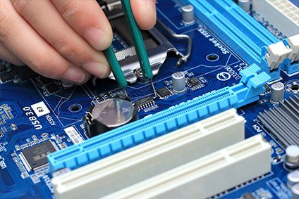
Plated through holes (PTH) usually realize the conductive connection between one side and the other side of the PCB panel in the thickness direction of the dielectric material (z-axis), or the connection between the conductor layers in the circuit of the multilayer board. The sidewalls of the vias are plated with copper to improve their conductivity.

However, the PTH copper plating process is neither conventional nor simple, and different processes may result in differences in the thickness of the copper plating layer. The method of PTH through-hole copper plating is usually electrolytic copper plating, that is, adding a layer of electroplated copper on the copper foil of the PCB material to realize the electrical connection of the through-hole. This virtually increases the thickness of the copper foil of the laminate, and introduces a change in the thickness of the copper foil throughout the material board. Variations in the thickness of the copper foil in a single board will cause differences in the thickness of the copper foil in the same board. Similarly, the uneven thickness of the copper foil between different boards will also reduce the repeatability of the same circuit between batches.
Because the wavelength of the signal decreases when the frequency is higher, the change in copper plating thickness has a greater impact on millimeter-wave circuits than low-frequency circuits. However, not all types of transmission lines are affected the same. For example, the amplitude and phase performance of RF/microwave microstrip transmission lines are only slightly affected by the thickness of PCB copper plating. However, circuits including grounded coplanar waveguide (GCPW) transmission lines and microstrip transmission line circuits with edge coupling characteristics will cause significant changes in their RF performance due to excessive changes in the thickness of the copper plating layer. Unless every change is taken into account, even with the best electromagnetic simulation software tools, the impact of PCB copper plating thickness on RF performance (for example, insertion loss and return loss) cannot be accurately predicted.
The edge coupling circuit achieves different degrees of coupling through a very narrow gap between the coupling conductors. Due to the microscopic size of the gap, the width of the gap between the coupled sidewalls will change due to the thickness of the copper plating. Loosely coupled circuits (larger gaps) are less affected by changes in copper plating thickness. As the gap between the coupled lines becomes narrower, the degree of coupling increases, and the influence of dimensional tolerances on the variation of copper plating thickness increases. For edge-coupled circuits with thicker copper layers, the sidewalls of the circuit transmission lines will also be higher. The difference in the height of the sidewalls will also lead to the difference in the coupling coefficient, and the effective dielectric constant (Dk) obtained by the circuit with different copper plating thickness will also be different.
Trapezoid effect
Changes in copper plating thickness will also affect the physical form of high-frequency circuit conductors. For modeling purposes, it is usually assumed that the conductor is rectangular. From the cross-sectional view, the width of the conductor is consistent along the length of the conductor. However, this is the ideal situation. The actual conductor usually has a trapezoidal shape, with the largest size at the bottom of the conductor, that is, at the junction of the conductor and the circuit dielectric substrate. For circuits with thicker copper, the trapezoidal shape becomes more serious. Changes in the size of conductors will cause changes in the current density through the conductors, which will result in changes in the performance of high-frequency circuits.
The impact of this change on circuit performance is different due to different circuit designs and transmission line technologies. The electrical performance of the standard microstrip transmission line circuit hardly changes greatly due to the trapezoidal effect of the conductor, but the circuit with edge coupling characteristics will have a significant impact due to the trapezoidal conductor, especially in the thicker copper layer. This effect becomes more obvious.
For edge-coupled circuits with tight coupling characteristics, computer modeling based on ideal rectangular conductors shows that there is a higher current density on the sidewalls of the coupled conductors. However, if you change the conductor model to a trapezoidal conductor, it will show that a greater current density appears at the bottom of the conductor, and the current density will increase as the thickness of the conductor increases.
As the current density changes, the electric field strength of the trapezoidal conductor also changes accordingly. For rectangular edge-coupled conductors, the current density along the coupling sidewalls is high, and a large part of the electric field around the conductors is in the air between the conductors. For edge-coupled conductors with a trapezoidal shape, the current density on the sidewalls is lower, and the electric field occupied by the air between the coupled conductors is less. The Dk of air is 1. An edge-coupled circuit with a rectangular conductor in the air with more electric fields between conductors will result in an effective Dk lower than that of a circuit with trapezoidal conductors, which has more surrounding conductors and dielectric materials. electric field.
Due to the standard PCB manufacturing process, the thickness of the copper plating on the PCB may change within a single circuit board, and the circuit performance of these copper thickness changes will also change according to the circuit topology and frequency. At millimeter wave frequencies, the size/wavelength of the circuit is small, and the influence of thickness changes is significant. Therefore, when using circuit simulation software to simulate the performance of a given circuit material, it is not only necessary to strictly control the Dk performance, but also to analyze and consider the changes and effects brought about by these processing techniques in advance.