PCB plays a very critical role in electronic equipment, so a robust defect detection strategy of one hour is required to ensure that any costly errors are avoided. This is true whether it is a bare PCB board or a fully assembled circuit board. Let us examine these two aspects in more detail.
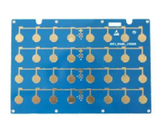
Defect detection strategy for prefabricated PCB
In essence, PCB manufacturing is a very precise science, with almost no room for error. Therefore, a major requirement is to verify the electrical continuity of the circuit board. There are two main methods to test these original boards. These include:
Needle bed test
Flying Probe Test System
Needle bed test
This way of working is to build a test fixture for a specific PCB design. The fixture contains a number of spring-loaded test pins. In fact, this is where the test is named. Press the PCB on the test pins, and then check their conductivity. This test is known for its short test time.

Flying probe test
Flying probe test originated from bare board test, involving short circuit, open circuit and other tests. The main parameter of the test is the resistance between points. However, these tests have been developed to measure capacitance and inductance. In fact, this is what makes them effective not only for testing bare circuit boards, but also for PCB components. The reasons why this test is widely used for defect detection include:
They are cost-effective.
Compared with ICT testers, they have fewer accessibility issues.
Since the movement of the probe is controlled by software, the modification is easy to implement.
Compared with ICT tests, they provide better test coverage.
Defect detection test can also benefit from the first article test. Essentially, this involves testing the first circuit board to build so-called "gold" cells. If the first article test does not show any defects, the entire production run is considered to have passed the connectivity test. Another important purpose of the first article is to establish the recording process of cardboard production. Once the POR is established and replicated, you can rest assured that the functions of each board are similar.
Therefore, for the first article inspection, it is necessary to check the following:
Measure and record all the properties of the circuit board, whether it is size or resistance. Once these values are verified through the design specifications, you can rest assured that the board is usable.
It is also important to check the clarity in the document.
For assembled boards, it is important to check whether the installed parts and materials meet the specified specifications.
These steps ensure that any defects can be identified in the first article stage itself, and then mass production is not carried out without classification. If any errors are found, corrective actions can be taken. At this stage, you can also determine any changes that may be required in the design.
If it is a bare PCB board, this is related or manual and automatic inspection technology. In short, the role of automatic optical inspection is to scan the board and then compare its image with the image of the first product production board. Therefore, any errors can be easily flagged. In addition, manual inspections are performed by trained technicians to determine any errors that may have been missed by the automated system after the bare board is manufactured.
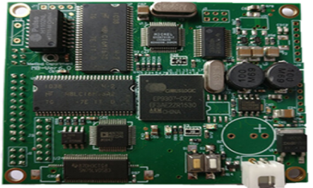
With so many checks and balances, experienced bare board manufacturers can significantly reduce the possibility of errors and defects on the bare PCB. The bare board can be used for the next step, including mounting components on the board or commonly known as PCB assembly.
Although we mainly discuss PCB bare board manufacturing and determine the defect detection strategy of the bare board, it is prudent to briefly understand some defect detection strategies of PCB components. Some of these include:
vision check
automatic inspection
Flying probe test
online test
function test
It is important to ensure that the PCB design is optimized for manufacturability. In this case, you may encounter many problems, such as solder defects and broken tombstones. A PCB manufacturer with a good track record can go a long way in helping you with robust design principles and also adhering to DFM rules and processes.