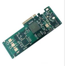
The basic production process of PCB
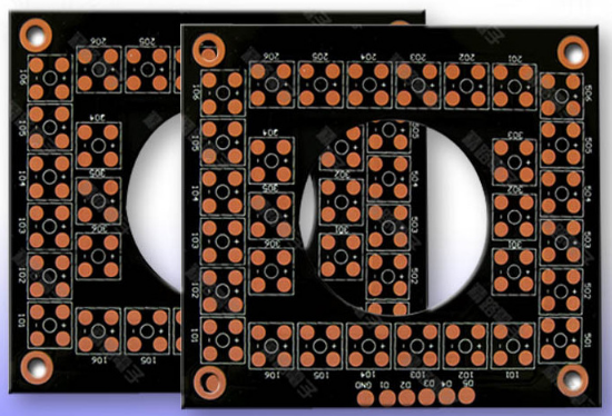
1. After the customer's original data processing of the PCB is completed, it is determined that there is no problem and the process capability is met, and the first stop is entered, according to the work order issued by the engineer to determine the size of the PCB substrate, the material of the PCB, and the number of layers ……When the material is sent out, in simple terms, it is to prepare the materials needed to make the PCB.
2. Dry film of inner layer board. Dry Film: It is a kind of resist that can photosensitize, develop, resist electroplating and resist etching. The photoresist is attached to the clean board surface by hot pressing. The water-soluble dry film is mainly due to its composition containing organic acid radicals, which will react with strong bases to become organic acid salts, which can be dissolved in water. It forms a water-soluble dry film, which is developed with sodium carbonate and stripped with dilute sodium hydroxide. The imaging action completed by the film. The surface of the PCB that is about to be processed in this step is "sticked" to a water-soluble dry film that undergoes a photochemical reaction, which can be exposed to light to show the prototype of all the circuits on the PCB.
3. Exposure The copper plate after pressing the film, cooperate with the PCB to make the negative film, and then expose it after automatic positioning by the computer, so that the dry film on the plate surface will be hardened due to the photochemical reaction, so as to facilitate the subsequent copper etching. Exposure intensity and exposure time
4. Development of the inner layer board Remove the unlighted dry film with a developer solution, leaving the exposed dry film pattern
5. Acid etching The exposed copper is etched to obtain the PCB circuit.
6. Remove the dry film. In this step, wash off the hardened dry film attached to the surface of the copper plate with a chemical solution, and the entire PCB circuit layer is now roughly formed
7. AOI uses automatic optical alignment inspection to check the correct PCB data to check whether there is a circuit breaker, etc. If this happens, check the PCB situation again.
8. Blackening This step is to treat the copper on the surface of the PCB that has been repaired and confirmed to be correct with a chemical solution to make the copper surface fluffy and increase the surface area to facilitate the adhesion of the two PCB layers
9. Pressing Pressing Use a hot pressing machine to press a steel plate on the PCB. After a certain period of time, the thickness is reached and the complete bonding is confirmed, the bonding work of the two PCB layers is now completed.
10. Drilling After inputting the engineering data into the computer, the computer will automatically locate and exchange for drills of different sizes for drilling. Since the entire PCB has been packaged, X-RAY scanning is required to find the positioning holes and then drill the holes necessary for the drilling procedure.
11. PTH Since there is no conduction between the layers in the PCB, copper should be plated on the drilled holes for interlayer conduction, but the resin between the layers is not conducive to copper plating, and a thin layer must be produced on the surface The chemical copper is then subjected to the copper plating reaction to meet the functional requirements of PCB.
12. Pre-treatment of the outer laminate film After drilling and through-hole plating, the inner and outer layers are connected, and then the outer layer is made to complete the circuit board. Laminating The same as the previous laminating step, the purpose is to make the outer layer of the PCB.
13. Outer layer exposure same as previous exposure steps
14. Outer layer development Same as the previous development step
15. Circuit etching The outer circuit is formed in this process
16. Remove the dry film. Remove the dry film. In this step, the hardened dry film attached to the surface of the copper plate is washed away with a chemical solution, and the entire PCB circuit layer has been roughly formed.
17. Spraying Spray the appropriate concentration of green paint evenly on the PCB board, or use a scraper and screen to evenly coat the ink on the PCB board.
18.S/M uses light to harden the parts that need to be kept green, and the parts that are not exposed to light will be washed away during the development process
19. Development: Wash away the unexposed hardened part with water, leaving the hardened part that cannot be washed away. Bake the top green paint to dry, and make sure that it is firmly attached to the PCB.
20. Printed text Printed text The correct text is printed on the appropriate screen according to customer requirements, such as material number, manufacturing date, part location, manufacturer and customer name and other information.
21. Tin spraying In order to prevent oxidation of the bare copper surface of the PCB and maintain good solderability, the board factory needs to perform surface treatments on the PCB, such as HASL, OSP, chemical immersion silver, nickel immersion gold...
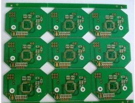
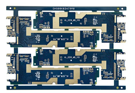
22. Forming Use a CNC milling cutter to cut the PCB of the large Panel into the size required by the customer.
23. Test 100% circuit test is performed on the PCB board for the performance required by the customer to ensure that its functionality meets the specifications.
24. Final inspection For the boards that have passed the test, 100% of the appearance will be inspected according to the customer's appearance inspection specifications.
25. Packaging
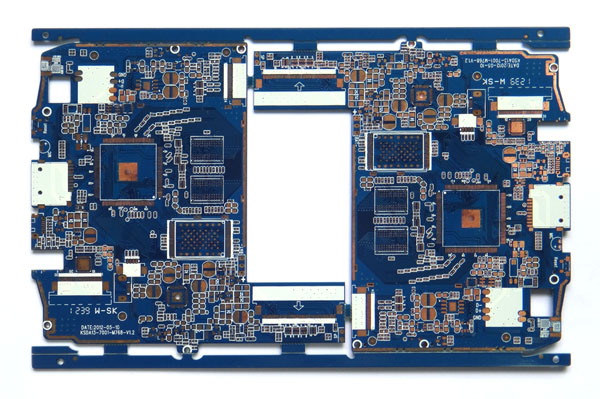
The copying procedure of the multi-layer board is the same as the single and double-sided board, it is nothing more than repeating the copying of several double-sided boards.
As an old driver in the copy board industry, I will mainly talk about some tips for copying multi-layer boards. It can also be regarded as a summary of the experience of copying boards over the years.
1. After copying the top and bottom layers, sand with sandpaper to grind out the inner layer. When sanding, the board must be pressed and laid flat, so that the sand is even.
If the board is very small, you can also spread the sandpaper flat. Use a finger to hold the board and rub it on the sandpaper. Of course, it is still necessary to flatten it so that it can be worn evenly.
2. There are two steps to explain the knowledge about the integration of each layer of the multilayer board in the copying software, one is scanning, and the other is the operation in the copying software.
Let's talk about scanning first. Generally, the side with more characters is scanned first, which is often called the top layer.
Transfer the top-level picture into Quickpcb, copy out all its elements, complete the top-level copy board work, and save the B2P file.
Then turn the PCB over and scan its reverse side, which is the bottom layer;
Because of the flipping action just now, the image obtained will be opposite to the top layer, so go to PHOTOSHOP to mirror the bottom layer image, that is, flip it back again, so that the top and bottom layers will not be at odds.
Then transfer the processed bottom-level picture into the copy board software, open the previously saved B2P file, and show all the top-level elements in front of you.
At this time, the B2P file has holes, surface stickers, lines, silk screens..., then open the layer setting window, close the top circuit layer and the top silk screen layer, leaving only multi-layer vias.
Then you can see the surface of the top layer and traces.
inner layer, and so on.