When choosing a PCB material, it is important to make the right choice for your design because the material affects the overall performance. Understanding how thermal and electrical characteristics affect your design before entering the manufacturing stage can save you time and money while achieving the best results.
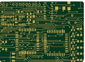
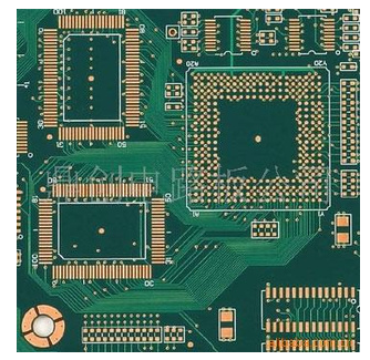
The PCB stack structure is to build a multi-layer PCB in a continuous sequence. The laminate is composed of magnetic core, prepreg and copper foil. Generally, the stacking is symmetrical. The board thickness of most products is less than 62 mils.
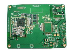
What material is used for the circuit board?
PCB material selection: electrical and manufacturing considerations
PCB materials: foil, core and prepreg
Use the following 3 items to manufacture printed circuit boards:
Prepreg: B-stage material, which is sticky and allows the bonding of different laminates or foils
Copper foil: used as a conductor in the PCB.
Copper Clad Laminate (Core): Laminated and cured by prepreg and copper foil.
Basic characteristics of dielectric materials
We know that PCB laminates are made of dielectric materials. When choosing a laminate, we need to consider the various characteristics of the dielectric material used.

Thermal performance:
Glass transition temperature (T g): The glass transition temperature or T g is the temperature range at which the substrate changes from a glassy, rigid state to a softened, deformable state as the polymer chain becomes more mobile. When the material cools down, its characteristics will return to its original state. T g is expressed in degrees Celsius (°C).
Decomposition temperature (T d ): The decomposition temperature or T d is the temperature at which the PCB material undergoes chemical decomposition (the material loses at least 5% of its mass). Like T g, T d is also expressed in degrees Celsius (°C).
Thermal conductivity (K): Thermal conductivity, or k, is the property of a material to conduct heat; low thermal conductivity means low heat transfer, and high conductivity means high heat transfer. The heat transfer rate is measured in watts per meter per degree Celsius (W/M °C).
Coefficient of Thermal Expansion (CTE): The coefficient of thermal expansion or CTE is the expansion rate of the PCB material when heated. CTE is expressed in parts per million (ppm) per heating degree Celsius. When the temperature of the material rises above T g, the CTE also rises. The CTE of the substrate is usually much higher than that of copper, which can cause interconnection problems when the PCB is heated.
Electrical characteristics:
Dielectric constant (E r or D k): Considering the dielectric constant of the material is very important for the consideration of signal integrity and impedance, which is a key factor in high-frequency electrical performance. The Er of most PCB materials is in the range of 2.5 to 4.5.
The values in the data sheet are only valid for the specific (usually 50%) resin content percentage in the material. The actual percentage of resin in the core material or prepreg varies with the composition, so D k will vary. The copper percentage and the thickness of the extruded prepreg will ultimately determine the media height. The dielectric constant generally decreases with increasing frequency.
Loss tangent (tanδ) or loss factor (D f ): Loss tangent or loss factor is the tangent of the phase angle between the resistive current and the reactive current in the dielectric. The dielectric loss increases as the value of D f increases. A low value of D f results in a "fast" substrate, while a large value results in a "slow" substrate. D f increases slightly with frequency; for high-frequency materials with a very low D f value, its change with frequency is very small. The value range is from 0.001 to 0.030.
Normal speed and loss: Normal speed material is the most common PCB material-FR-4 series. Their dielectric constant (D k) and frequency response are not very flat, and they have a higher dielectric loss. Therefore, their applicability is limited to a few GHz digital/analog applications. An example of this material is Isola 370HR.
Medium speed and loss: Medium speed materials have a flatter D k vs. frequency response curve, and dielectric loss is about half of normal speed materials. These are suitable for up to ~10GHz. An example of this material is Nelco N7000-2 HT.
High speed and low loss: These materials also have a flatter D k and frequency response curve and low dielectric loss. Compared with other materials, they also produce less harmful electrical noise. An example of this material is Isola I-Speed.
Very high speed and very low loss (RF/microwave): The materials used for RF/microwave applications have the flattest D k and frequency response and the smallest dielectric loss. They are suitable for applications up to ~20GHz. An example of this material is Isola I-Tera MT40 and Tachyon 100G.
Signal loss and operating frequency
PCB materials can affect the signal integrity of high-frequency circuits. You can minimize the attenuation on the circuit board by choosing the correct PCB substrate and copper foil. When it comes to signal loss in PCBs, these two materials play a very important role. Signal loss includes dielectric loss and copper loss.
Dielectric loss
Dielectric materials are composed of polarized molecules. These molecules vibrate in the electric field created by the time-varying signal on the signal trajectory. This heats up the dielectric and causes the dielectric loss part of the signal loss. This signal loss increases with increasing frequency. The use of materials with a lower dissipation factor can minimize signal loss. The higher the frequency, the greater the loss of any given material. This is due to the constantly changing electromagnetic field causing molecular vibrations in the dielectric material. The faster the molecule vibrates, the greater the loss.
Copper loss
Copper loss is essentially related to the current flowing through the conductor. Electrons may not always flow through the center of the conductor. If the copper trace is completed with nickel, most of the current may flow through the nickel layer. As the frequency increases, the skin effect loss will become greater. This can be compensated by increasing the width of the trace, which in turn creates a larger surface area. Wider traces always have lower skin effect losses. The profile of the copper foil-dielectric tooth interface increases the effective length, thereby increasing the copper loss. It is always recommended to use thin or very thin copper.
In order to better choose PCB materials, the table below divides the basic materials into different categories according to signal loss characteristics.
PCB material selection: electrical and manufacturing considerations
PCB material category comparison of loss tangent at 10 GHz
On the left, we have materials like FR-4. These are standard and easy-to-process everyday materials that can be used for any application. But they are also the most lossy laminates. It may also have a large number of other electrical and mechanical problems. Materials such as Isola I-speed, Isola Astra and Tachyon exhibit low loss at high frequencies.
Copper foil selection
The following are several characteristics that we need to consider when choosing copper foil:
Copper thickness: Typical thicknesses range from 0.25 ounces (0.3 mils) to 5 ounces (7 mils).
Copper purity: It is the percentage of copper in the copper foil. The purity of electronic grade copper foil is about 99.7%.
Copper dielectric interface profile: Thin type has low signal copper loss at high frequency.
Copper foil type
Copper electroplating: This copper has a vertical grain structure and a rougher surface. Electroplated copper is usually used for rigid PCBs.
Calendered copper: A type of copper that is made very thin by processing between heavy rollers and is widely used in the production of flexible PCBs. Calendered copper has a horizontal texture structure and a smoother surface, which makes it an ideal choice for rigid-flexible and flexible PCBs.
Best Practices for PCB Material Selection
Thermal expansion matching coefficient (CTE): CTE is the most critical thermal characteristic of the substrate. If the components of the substrate have different CTEs, they may expand at different rates during the manufacturing process.
Choose a compact base structure: the D k distribution in a compact base structure will be uniform.
Avoid the use of FR (flame retardant)4 in high frequency applications: This is due to its high dielectric loss and steeper D k vs. frequency response curve. (For frequencies below 1 GHz).
Use less hygroscopic materials: Hygroscopicity is the ability of the PCB material (in this case copper) to resist water absorption when immersed in water. It is the percentage increase in weight of PCB material due to water absorption under controlled conditions according to standard test methods. Most materials have moisture absorption values in the range of 0.01% to 0.20%.
Always use CAF-resistant materials: Conductive anode filament (CAF) is a metal filament formed by an electrochemical migration process that is known to cause PCB failure. Using anti-CAF materials is one of the most effective ways to prevent the formation and failure of CAF.