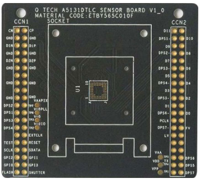
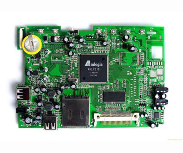
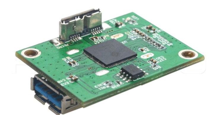
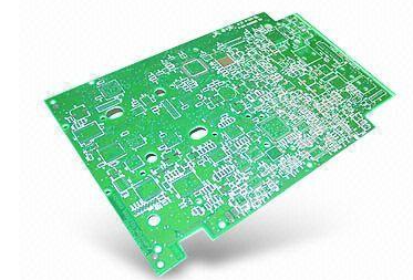
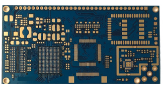
As the carrier of various components and the hub of circuit signal transmission,PCB circuit board has become the most important and key part of electronic information products. Its quality and reliability level determine the quality and reliability of the whole equipment.
PCB
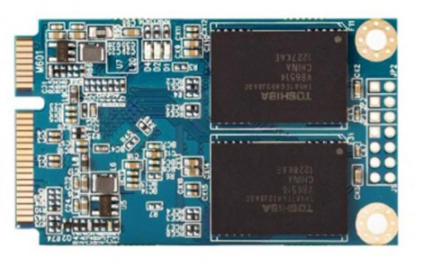
With the miniaturization of electronic information products and the environmental protection requirements of lead-free and halogen-free, PCBs are also developing in the direction of high density, high Tg and environmental protection. However, due to cost and technical reasons, a large number of failure problems have occurred in the process of PCB production and application, which has caused many quality disputes. In order to clarify the cause of the failure in order to find a solution to the problem and distinguish the responsibilities, it is necessary to conduct a failure analysis on the failure cases that have occurred.
Basic procedure of failure analysis

To obtain the accurate cause or mechanism of PCB failure or failure, the basic principles and analysis process must be followed, otherwise valuable failure information may be missed, causing the analysis to be unable to continue or may get wrong conclusions. The general basic process is that, first, based on the failure phenomenon, the failure location and failure mode must be determined through information collection, functional testing, electrical performance testing, and simple visual inspection, that is, failure location or failure location.
For simple PCB or PCBA, the failure location is easy to determine, but for more complex BGA or MCM packaged devices or substrates, the defects are not easy to observe through a microscope and are not easy to determine for a while. At this time, other means are needed to determine.
As the carrier of various components and the hub of circuit signal transmission, PCB has become the most important and critical part of electronic information products. The quality and reliability of PCB determine the quality and reliability of the whole equipment.
With the miniaturization of electronic information products and the environmental protection requirements of lead-free and halogen-free, PCBs are also developing in the direction of high density, high Tg and environmental protection. However, due to cost and technical reasons, a large number of failure problems have occurred in the production and application of PCBs, which has caused many quality disputes. In order to clarify the cause of the failure in order to find a solution to the problem and distinguish the responsibilities, it is necessary to conduct a failure analysis on the failure cases that have occurred.
Basic procedure of failure analysis
To obtain the accurate cause or mechanism of PCB failure or failure, the basic principles and analysis process must be followed, otherwise valuable failure information may be missed, causing the analysis to be unable to continue or may get wrong conclusions. The general basic process is that, first, based on the failure phenomenon, the failure location and failure mode must be determined through information collection, functional testing, electrical performance testing, and simple visual inspection, that is, failure location or failure location.
For simple PCB or PCBA, the failure location is easy to determine, but for more complex BGA or MCM packaged devices or substrates, the defects are not easy to observe through a microscope and are not easy to determine for a while. At this time, other means are needed to determine.