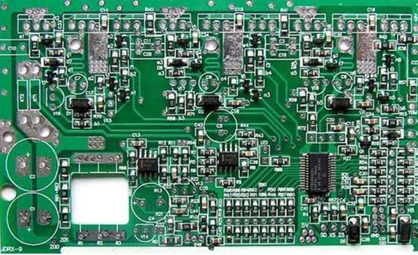
As the complexity of the devices they carry increases, PCB design becomes more and more complex. For quite a long time, circuit design engineers have been doing their own design without incident, and then transfer the completed circuit diagram design to the PCB design engineer. After the PCB design engineer completes his work independently, he transfers the Gerber file to PCB manufacturing. factory. The work of circuit design engineers, PCB design engineers, and PCB manufacturers are all isolated from each other, and there is little communication.
The first step of PCB design is in the concept phase. At this time, the circuit design engineer should conduct a technical evaluation together with the PCB design engineer. This assessment should consider the following questions:
1. What devices are used?
2. Which package is used for the device? What is the number of pins? What is the pin configuration?
3. Based on the trade-off of cost and performance, how many layers of PCB should be used?
4. What are the target values of parameters such as clock frequency and signaling speed?

In addition, design engineers should also consider factors such as bus architecture, whether to use parallel or serial connections, and impedance matching strategies. When the impedance is not matched, reflections, ringing and other undesirable interference will occur.
For the current PCB design, it is best to do everything according to the rules. In the past, it was constrained by manufacturing issues, but now when engineers try to reduce the size of the PCB and still make it manufacturable, everything is subject to complex constraints. Although design requirements may cause a lot of constraints, it is also important not to allow the design to be overly constrained. Compared with simply designing with constraints, it is wiser to learn more from simulation and analysis.
Simulation is the key
Once the circuit is designed and the schematic is drawn, it is time to perform functional verification, which is usually completed with simulation tools. The purpose of simulation is not to replace physical prototype generation, but to avoid repeated generation of prototypes, because simulation enables design engineers to discover design flaws that generally cannot be discovered until the prototype is generated.
In the simulation process, various design topologies can be tried and replaced with devices from different manufacturers to verify their impact on circuit performance. However, in the simulation, there are endless problems with the usability and validity of the model. At present, all commonly used PCB design toolkits have expensive model libraries, but it may happen that a particular device is not in the library more than once. However, device suppliers generally solve this problem by launching Spice models on their website, so it is a good idea to find them on the device supplier's website.
Limitations of circuitous wiring
But Spice-based simulation also has limitations. It can generate idealized simulation signals that do not necessarily represent real conditions. The real signal may have noise and phase shifts that change the realism.
Physical realization
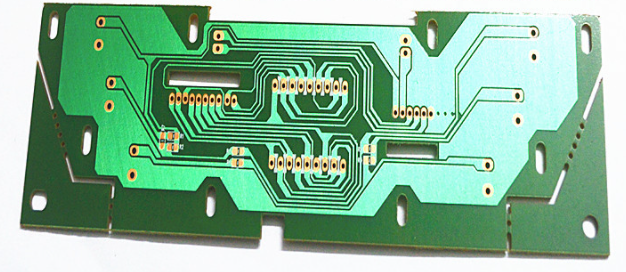
After the performance problems have been eliminated through simulation, the next step is to place and route the circuit to generate a physical prototype. Layout and routing must ensure that the circuit performance meets the design specification requirements, and ensure that the board shape matches the design shape parameters. At this time, it will be very necessary to cooperate with the mechanical engineer.
Design constraints
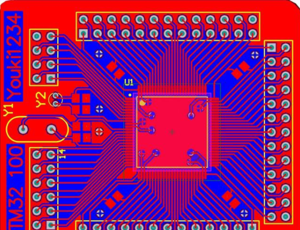
There are many challenges in PCB layout, the main one of which is to ensure that the constraints are met. These constraints are used to solve signal integrity issues, manufacturability issues, electromagnetic interference, thermal effects, or a combination of these issues.
In addition to design constraints, many factors related to current specific device technologies make PCB layout and routing more complicated. For example, advanced semiconductor packaging technologies such as chip-on-board (COB) can make routing extremely tricky. The current high-density package can hold more than 2,000 pins with a pin pitch of less than 0.65mm. This kind of package will bring great difficulties to managing I/O and signal speed, and Escape Routing for this kind of package is also a high-skill job.
PCB layout and routing of programmable logic devices is another challenge. Some high-end PCB design kits (such as the PCB design kits provided by Altium and Mentor Graphics) can be closely linked with the FPGA supplier's design tools and can be used to complete the integrated design of the FPGA and the PCB itself.
In the past, the pin configuration of large FPGAs was generally completed by FPGA design engineers, but the PCB layout and routing were not considered too much during the configuration. People now realize that FPGAs with programmable I/O are the source of traces in and out. It is much easier to change the FPGA to cater to the PCB layout than to change the PCB to match the FPGA's I/O settings.
Final check
The final step before taking the PCB layout for manufacturing is the final inspection. The signal integrity and timing must be checked to ensure that the signal reaches the destination in time and has sufficient quality assurance. Design constraint conflicts will be revealed at this time, and this has to be weighed.
At the end of the PCB design, manufacturing data must be generated, including all documents related to production, assembly and testing. Throughout the design process, there must be sufficient communication between design team members and the manufacturer to understand the manufacturer’s technical capabilities and limitations. In addition, the manufacturing data must be verified so that the design engineer has the last chance to find errors.