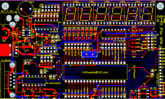
As the carrier of various components and the hub of circuit signal transmission, PCB has become the most important and vital part of electronic information products. The quality and reliability of the PCB determines the quality and reliability of the entire equipment. However, due to cost and technical reasons, a large number of failures occurred during the PCB production and PCB application.
For this kind of failure problem, we need to use some common failure analysis techniques to ensure the quality and reliability of the PCB during the manufacturing process. Ten main failure analysis techniques are summarized for reference.
1. Visual inspection
Visual inspection is to check the appearance of the PCB by visual inspection or using some simple instruments (for example, stereo microscope, metallographic microscope or even magnifying glass) to find the part failure and related physical evidence. The main function is to locate the fault and initially determine the failure mode of the PCB.

The appearance inspection mainly checks the PCB pollution, corrosion, the position of the exploded board, the regularity of circuit wiring and failure. If it is batch or single, it is always concentrated in a certain area and so on. In addition, there are many PCB failures that can only be discovered after assembly into PCBA. Whether the failure is caused by the assembly process and the influence of the materials used in the process also requires careful examination of the characteristics of the failure area.
2. X-ray fluoroscopy
For some parts that cannot pass the visual inspection, as well as through holes and other internal defects inside the PCB, we must use an X-ray fluoroscopy inspection system to inspect. X-ray fluoroscopy systems use different material thicknesses or different material densities to absorb X-rays or transmit light through different principles. This technology is more used to check the defects inside PCBA solder joints, the defects inside the through holes, and the position of the defective solder joints of high-density packaging BGA or CSP devices. The resolution of current industrial X-ray fluoroscopy equipment can reach less than one micron, and it has been transformed from a two-dimensional imaging device to a three-dimensional imaging device. Even five-dimensional (5D) equipment has been used for packaging inspection, but this type of 5D X fluoroscopy system is very expensive and rarely finds practical application in the industry.
3. Slice analysis
Slicing analysis is through a series of methods and steps (such as sampling, inlaying, slicing, polishing, etching, and observation. Through slicing analysis, you can obtain rich information about the PCB microstructure (through holes, plating, etc.), which is the next step The quality improvement provides a good foundation. However, this method is destructive. After sectioning, the sample will be destroyed. At the same time, this method requires a lot of sample preparation, and sample preparation takes a long time, which requires well-trained techniques Personnel to complete.
4. Scanning acoustic microscope
At present, the C-mode ultrasound scanning acoustic microscope is mainly used for electronic packaging or assembly analysis. It uses high-frequency ultrasonic reflection on the discontinuous interface between the material and the phase and pole. The imaging method is based on the change of the image, while the scanning method is to scan the information in the XY plane along the Z axis. Therefore, the scanning acoustic microscope can be used to detect various defects in components, materials, and PCBs and PCBAs, including cracks, delaminations, inclusions and voids. If the frequency width of the scanning sound is large enough, the internal defects of the solder joints can also be directly detected. The typical scanning sound image is a red warning color, indicating a defect. Since many plastic packaged components are used in the SMT process, a large number of problems that are sensitive to moisture reflow will occur in the process of converting lead to lead-free. That is, when the hygroscopic plastic packaging device is reflowed at a higher lead-free process temperature, there will be internal or substrate delamination and cracking, and ordinary PCBs are often cracked at the high temperature of the lead-free process. At this time, the scanning acoustic microscope highlights its special advantages in the non-destructive testing of multilayer high-density PCBs. Usually, only by visual inspection can the obvious rupture plate be found.
5. Micro infrared analysis
Micro-infrared analysis is an analysis method that combines infrared spectroscopy and microscopy. It uses different materials (mainly organic substances) to absorb infrared spectra with different absorption rates. Principle: Analyze the chemical composition of the material and combine it with a microscope to make visible light and infrared light have the same optical path. As long as it is in the visible field of view, trace organic pollutants can be found for analysis. If a microscope is not used, usually infrared spectroscopy can only analyze a large number of samples. In many cases in electronic processes, trace contamination can cause poor solderability of PCB pads or pins. It is conceivable that it is difficult to solve the process problem without the infrared spectrum of the microscope. The main purpose of micro-infrared analysis is to analyze the organic contaminants on the welding surface or joint surface, and analyze the reasons for corrosion or poor solderability.