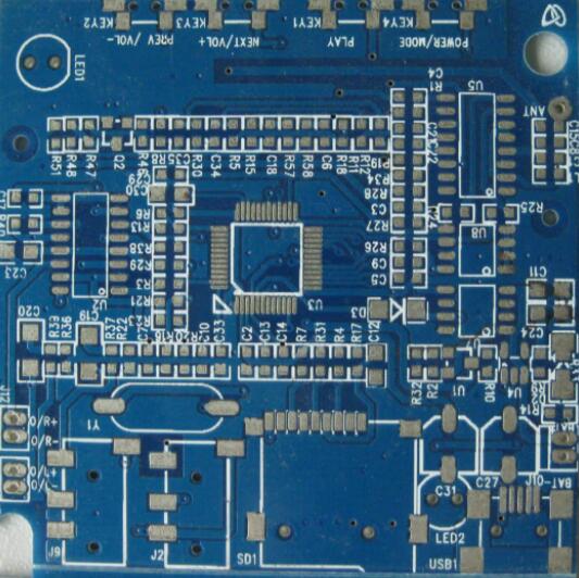
In circuit PCB design, we are generally concerned about the quality of the signal, but sometimes we are often limited to the signal line research, and the power supply and ground as the ideal situation to deal with, although this can make the problem simplified, but in high-speed design, this simplification is not feasible. Although the more direct result of circuit design is the expression of signal integrity, we must not therefore ignore the power supply integrity design. Power supply integrity directly affects the signal integrity of the final PCB board. Power supply integrity and signal integrity are closely related, and in many cases, the main cause of signal distortion is the power supply system. For example, the ground rebound noise is too large, the design of decoupling capacitor is inappropriate, the influence of the loop is very serious, the segmentation of the ground plane of multi-power supply is not good, the stratum design is unreasonable, the current is not uniform and so on.
1) Power distribution system
Power supply integrity design is very complicated, but how to control the impedance between power supply system (power supply and ground plane) is the key to design. In theory, the lower the impedance between power systems, the better, the lower the impedance, the smaller the noise amplitude, the smaller the voltage loss. In practical design, we can determine the target impedance we hope to achieve by specifying the maximum voltage and power supply variation range, and then adjust the relevant factors in the circuit to make the impedance of each part of the power supply system (and frequency related) target impedance to approximate.

2) To bounce
When the edge rate of high-speed devices is less than 0.5ns, the data exchange rate from the large-capacity data bus is particularly fast, and the power supply instability problem occurs when it produces strong ripples in the power supply layer that affect the signal. When the current through the ground loop changes, because the circuit inductance will produce a voltage, when the rising edge shortens, the rate of current change increases, the ground rebound voltage increases. At this point, the ground plane (ground) is not ideal zero level, and the power supply is not ideal DC level. As the number of simultaneous switching gates increases, ground bounce becomes more severe. For a 128-bit bus, there may be 50_100 IO lines switching along the same clock. In this case, the inductance feedback to the power supply and ground loop of the IO driver switched at the same time must be as low as possible, otherwise, the stationary connected to the same ground will have a voltage brush. Ground bounce can occur anywhere, such as on chips, packages, connectors, or circuit boards, resulting in power integrity problems.
From a technology development perspective, the rising edge of the device will only decrease and the width of the bus will only increase. The only way to keep ground bounce acceptable is to reduce the power supply and ground distribution inductance. For the chip, that means moving to an array chip, placing as much power and ground as possible, and making the wires to the package as short as possible to reduce inductance. For encapsulation, this means moving layer encapsulation so that the ground planes of the power supply are more closely spaced, as used in BGA encapsulation. For connectors, this means using more ground pins or redesigning the connector to have an internal power supply and ground plane, such as a linker-based ribbon cord. For a circuit board, this means making the adjacent power supply and ground plane as close as possible. Since inductance is proportional to length, making the connection between power supply and ground as short as possible will reduce ground noise.
3) Decoupling capacitance
Between power supply and to add some capacitance can reduce the noise of the system, but exactly how much capacitance on the circuit board capacity of each capacitance value how suitable each capacitor in what position better like we usually did not go to seriously consider these problems, only by the designer's experience, sometimes even think capacitance as little as possible. In the design of high speed, we must consider the parasitic capacitance parameter, quantitative calculate the number of decoupling capacitors and the capacity value of each capacitor and placement of specific position, ensure that the impedance of the system in the range of control, a basic principle is the need of decoupling capacitor, one can't be little, excess capacity.