Printed circuit board disassembly method
1. The circuit board factory disassembles the components on the single-sided printed circuit board: toothbrush method, screen method, needle method, tin suction device, pneumatic suction gun, etc. can be used. Table 1 compares these methods in detail.
Most simple and convenient methods for disassembling electronic components (including foreign advanced pneumatic sniffer) are only suitable for single panel, and the effect is not good for double panel and multi panel.
2. Disassemble the components on the double-sided printed circuit board: single-side integral heating method, needle tube hollowing method, tin flow soldering machine can be used. The single-link integral heating method requires special heating tools, which is inconvenient for general use. Needle tube hollowing method: first cut off the pins of the components that need to be disassembled, and remove the components. At this time, the pins of the components are left on the printed circuit board, and then each pin is removed with a soldering iron. The tin on the solder is melted, use tweezers to take it out until all the pins are taken out, and then use a medical needle that matches the inner diameter of the pad hole to hollow it out. Although this method requires several more processes, it is not suitable for printed circuit boards. There is no impact, it is convenient to obtain materials and easy to operate, and it is extremely easy to realize. After many years of practice, I think it is an ideal method.
3. Disassemble the components on the multi-sided printed circuit board: If the above methods (except tin flow soldering machine) are used, it is either difficult to disassemble, or it is easy to cause connection failures between layers. Generally, the soldering pin method is used to cut the component from the root of the component pin, leave its pin on the printed circuit board, and then solder the pin of the new device to the pin remaining on the printed circuit board. But it is not easy to weld multi-leg integrated blocks. The tin flow soldering machine (also known as the secondary soldering machine) can solve this problem and is the most advanced tool for disassembling the integrated blocks on the double and multilayer printed circuit boards. However, the cost is relatively high, requiring an investment of several thousand yuan. The tin flow soldering machine is actually a special small wave soldering machine. It uses a tin flow pump to extract fresh and unoxidized molten tin from the tin pot and gush out through the optional different specifications of spray nozzles to form a The local small wave peaks act on the bottom of the printed circuit board. The solder of the pins and solder holes of the removed components on the printed circuit board will melt immediately within 1 to 2 seconds. At this time, the Then use compressed air to blow through the solder holes of the component, re-insert the new component, and then solder the finished product on the wave crest of the spray nozzle.
Of course, in addition to the above, there are other methods (for example: copper wire method, alcohol lamp method, etc.), but because of its lack of outstanding features, it is similar to the method described above, so I won't talk about it here.

2. Double-sided circuit board welding techniques for circuit board welding
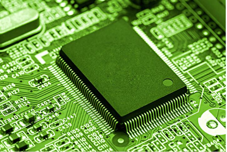
The difference between single-sided circuit boards and double-sided circuit boards is the number of copper layers. Double-sided circuit boards have copper on both sides of the circuit board, which can be connected through vias. However, there is only one layer of copper on one side, which can only be used for simple circuits, and the holes made can only be used for plug-in connections. The technical requirement of double-sided circuit boards is that the wiring density becomes larger, the hole diameter is smaller, and the hole diameter of the metallized hole is getting smaller and smaller. The quality of the metallized holes on which the layer-to-layer interconnection relies is directly related to the reliability of the printed board. With the shrinking of the pore size, the debris that did not affect the larger pore size, such as brush debris and volcanic ash, once left in the small hole will cause the electroless copper and electroplating to lose its effect, and there will be holes without copper and become holes. The deadly killer of metallization.
Welding method of double-sided circuit board
In order to ensure reliable electrical conduction of the double-sided circuit board, the connection holes on the double-sided board (that is, the through-hole part of the metallization process) should be welded with wires or the like first, and the protruding part of the connecting wire tip should be cut to avoid stabs. Injury to the operator's hand, this is the preparation for the wiring of the board.
The essentials of double-sided circuit board welding:
1. For devices that require shaping, they should be processed according to the requirements of the process drawings; that is, they must be shaped first and then plug-in.
2. After shaping, the model side of the diode should face up, and there should be no discrepancies in the length of the two pins.
3. When inserting devices with polarity requirements, pay attention to their polarity not to be reversed. Roll integrated block components, after inserting, no matter it is a vertical or horizontal device, there must be no obvious tilt.
4. The power of the soldering iron used for soldering is between 25~40W. The temperature of the soldering iron tip should be controlled at about 242 degree Celsius. If the temperature is too high, the tip is easy to "die", and the solder cannot be melted if the temperature is low. The soldering time should be controlled at 3 ~4 seconds.
5. During the formal welding, generally operate according to the welding principle of the device from short to high and from the inside out. The welding time should be mastered. If the time is too long, the device will be burnt, and the copper line on the copper clad board will also be burnt.
6. Because it is double-sided welding, a process frame or the like for placing the circuit board should also be made, so as not to squeeze the components underneath.
7. After the circuit board is soldered, a comprehensive check-in check should be carried out to check for missing insertion and soldering. After confirmation, trim the redundant device pins and the like on the circuit board, and then flow into the next process.
8. In the specific operation, the relevant process standards should be strictly followed to ensure the welding quality of the product.
With the rapid development of high technology, electronic products that are closely related to the public are constantly being updated. The public also needs electronic products with high performance, small size and multiple functions, which puts forward new requirements on circuit boards. This is why double-sided circuit boards were born. Due to the wide application of double-sided circuit boards, printed circuit board manufacturing has also become lighter, thinner, shorter, and smaller.