Layout is an important part of PCB design, and it is also the most time-consuming part of the whole PCB design. Engineers need to follow some basic rules, such as chamfering rules, 3W rules, etc.
Ground circuit rules
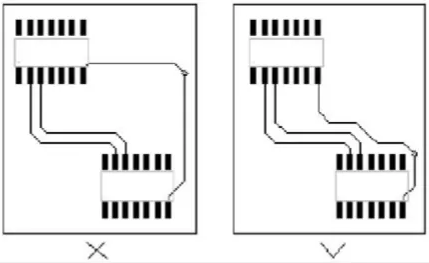
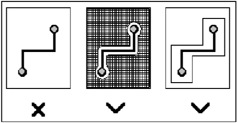
The corresponding ground circuit rule is actually to minimize the loop area of the signal, which is often seen in some important signals, such as clock signal and synchronous signal;
Crosstalk refers to the mutual interference caused by long parallel wiring between different networks on PCB, mainly due to the distributed capacitance and inductance between parallel lines. The main measures to overcome crosstalk are as follows:
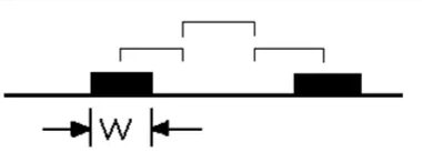
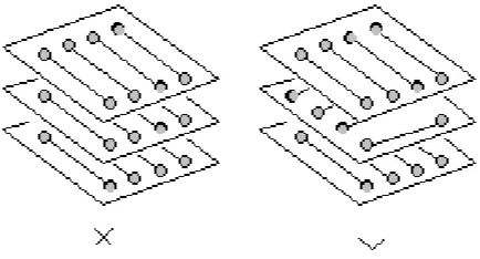
The direction control rule of routing, that is, the routing direction of adjacent layers is orthogonal structure. Different signal lines should be avoided to go in the same direction in the adjacent layers to reduce unnecessary inter layer interference; when this situation is difficult to avoid due to board structure constraints (such as some back boards), especially when the signal rate is high, it should be considered to isolate the wiring layers with the ground plane and isolate the signal lines with the land signal lines.
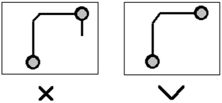
Generally, floating wiring at one end is not allowed(Dangling Line),It is mainly to avoid "antenna effect" and reduce unnecessary interference radiation and acceptance, otherwise it may bring unpredictable results.
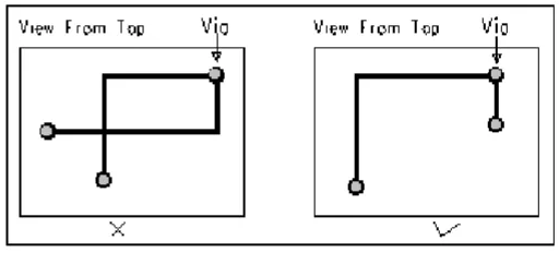

Device decoupling rules
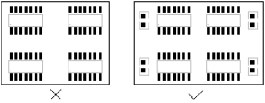
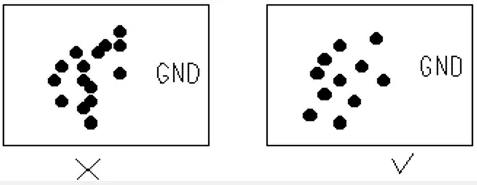
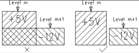

Because the electric field between the power layer and the stratum is variable, electromagnetic interference will radiate from the edge of the plate. It's called edge effect.
The solution is to shrink the power layer, so that the electric field is only conducted in the range of the ground plane. Taking an H (dielectric thickness between power supply and ground) as a unit, if the electric field is indented by 20h, 70% of the electric field can be limited to the edge of the ground plane, and the electric field of 98% can be limited to within 100h.
Other precautions for PCB layout
1. General rules
1.1 digital, analog and DAA signal wiring areas are pre divided on the PCB.
1.2 digital and analog components and corresponding wiring shall be separated as far as possible and placed in their respective wiring areas.
1.3 high speed digital signal routing shall be as short as possible.
1.4 sensitive analog signal routing shall be as short as possible.
1.5 reasonably distribute power and ground.
1.6 DGND, agnd and field separation.
1.7 wide wires shall be used for power supply and critical signal routing.
1.8 the digital circuit is placed near the parallel bus / serial DTE interface, and the DAA circuit is placed near the telephone line interface.
Basic rules and skills of PCB wiring
2. Placement of components
2.1 in the system circuit schematic diagram:
a) Divide digital, analog, DAA circuits and their related circuits;
b) Divide digital, analog and hybrid digital / analog components in each circuit;
c) Pay attention to the positioning of power supply and signal pins of each IC chip.
2.2 preliminarily divide the wiring area of digital, analog and DAA circuits on PCB (generally 2 / 1 / 1). Digital and analog components and their corresponding wiring shall be far away from and limited in their respective wiring area as far as possible.
Note: when DAA circuit accounts for a large proportion, there will be more control / status signal routing through its wiring area, which can be adjusted according to local rules, such as component spacing, high voltage suppression, current limitation, etc.
2.3 after preliminary division, place components from connector and Jack:
a) Place plug-ins around connector and jack;
b) Leave space for power supply and ground wiring around components;
c) Place the corresponding plug-in around the socket.
2.4 first place hybrid components (such as modem devices, a / D, D / a conversion chips, etc.):
a) Determine the placement direction of components, and try to make the digital signal and analog signal pins face their respective wiring areas;
b) Place components at the junction of digital and analog signal wiring area.
2.5 place all simulators:
a) Place analog circuit components, including DAA circuit;
b) The simulators are close to each other and placed on one side of the PCB containing txa1, TXA2, Rin, VC and VREF signal wiring;
c) Avoid placing high noise components around txa1, TXA2, Rin, VC and VREF signal wiring;
d) For serial DTE modules, DTE EIA / tia-232-e
The receiver / driver of the series interface signal shall be close to the connector as far as possible and away from the high-frequency clock signal routing, so as to reduce / avoid the increase of noise suppression devices on each line, such as choke and capacitance.
2.6 placing digital components and decoupling capacitors:
a) Digital components are placed in a centralized manner to reduce the wiring length;
b) Place a 0.1uF decoupling capacitor between the power supply / ground of the IC, and the connection route shall be as short as possible to reduce EMI;
c) For parallel bus module, the components are close to each other
The connector edge shall be placed to meet the application bus interface standard, such as the ISA bus routing length is limited to 2.5in;
d) For the serial DTE module, the interface circuit is close to the connector;
e) The crystal oscillator circuit shall be as close to its driver as possible.
2.7 the ground wire of each area is usually connected at one or more points with 0 ohm resistance or bear.
3. Signal routing
3.1 in modem signal routing, signal lines prone to noise and signal lines susceptible to interference shall be kept away as far as possible. If it is unavoidable, neutral signal lines shall be used for isolation.
The signal pin, neutral signal pin and signal pin vulnerable to interference of modem are shown in the table below:
Modem signal line
RS-232C serial port signals are divided into three categories: transmission signal, contact signal and ground wire
(1) Transmission signal: refers to TXD (transmission data signal line) and RXD (reception data signal line). The format of information transmitted via TXD and received via RXD is: a transmission unit (byte) is composed of start bit, data bit, parity bit and stop bit.
(2) Contact signal: refers to RTS, CTS, DTR, DSR, DCD and RI signals, and their functions are:
RTS (request transmission) is the contact signal sent by PC to modem. The high level indicates that the PC requests to transmit data to the modem
CTS (clear transmission) is the contact signal sent by modem to PC. High level indicates that the modem responds to the RTS signal sent by the PC and is ready to send data to the remote modem.
DTR (data terminal ready) is the contact signal sent by PC to modem. The high power screen indicates that the PC is ready, and a communication channel can be established between the local modem and the remote modem. If it is a low power screen, force the modem to terminate communication.
DSR (data device ready) is the contact signal sent by modem to PC. It indicates the working state of the local modem. A high level indicates that the modem is not in the test call state and can establish a channel with the remote modem.
DCD (transmission detection) is the status signal sent by modem to PC. High level indicates that the local DCE receives the carrier signal from the remote modem.
RI (ringing indication) is the status signal sent by modem to PC. High level indicates that the local modem receives the ringing signal from the remote modem.
(3) Ground wire signal (GND) provides the same potential reference point for the connected PC and modem.
56K high-speed modem is a dial-up high-speed modem launched in 1997. Its transmission rate is higher than the limit rate of 33.6kbps on the traditional telephone line because it adopts a modulation and demodulation technology completely different from 33.6k, and its workpiece principle and application requirements are also different from 33.6k high-speed modem.
The connection standards between DTE and DCE include cctv.10/x.26;
3.2 digital signal wiring shall be placed in the digital signal wiring area as far as possible;
Analog signal wiring shall be placed in the analog signal wiring area as far as possible;
(isolation wiring can be pre placed to limit the wiring to prevent the wiring from spreading out of the wiring area)
Digital signal routing is perpendicular to analog signal routing to reduce cross coupling.
3.3 use isolated routing (usually ground) to limit analog signal routing to analog signal wiring area.
a) The isolated ground wiring of the analog area surrounds the analog signal wiring area, which is arranged on both sides of the PCB board, with a line width of 50-100mil;
b) The isolated wiring of the digital area shall surround the digital signal wiring area, which shall be arranged on both sides of the PCB with a line width of 50-100mil, and the edge of one PCB shall be arranged with a width of 200mil.
3.4 parallel bus interface signal wiring line width "10mil (generally 12-15mil), such as / HCS, / HRD, / HWT, / reset.
3.5 analog signal wiring width: 10mil (generally 12-15mil), such as MICM, micv, spkv, VC, VREF, txa1, TXA2, RXa, Telin and telout.
3.6 the routing of all other signals shall be as wide as possible, the line width shall be 5MIL (generally 10mil), and the routing between components shall be as short as possible (it shall be considered in advance when placing components).
3.7 the wiring line width from bypass capacitor to corresponding IC shall be 25mil, and vias shall be avoided as far as possible.
3.8 signal lines passing through different areas (such as typical low-speed control / status signals) shall pass through isolated ground wire at one point (preferred) or two points. If the routing is only on one side, the isolated ground wire can go to the other side of the PCB to skip the signal routing and maintain continuity.
3.9 high frequency signal routing shall avoid 90 degree angle bending, and smooth arc or 45 degree angle shall be used.
3.10 high frequency signal wiring shall reduce the use of via connection.
3.11 all signal routing shall be away from the crystal oscillator circuit.
3.12 single continuous routing shall be adopted for high-frequency signal routing to avoid several sections of routing extending from one point.
3.13 in DAA circuit, leave at least 60mil of space around the perforation (all layers).
3.14 clear the ground loop to prevent accidental current feedback from affecting the power supply.
4. Power supply
4.1 determine the power connection relationship.
4.2 in the digital signal wiring area, 10uF electrolytic capacitor or tantalum capacitor is connected in parallel with 0.1uF ceramic chip capacitor and then connected between power supply / ground. Place one at the power inlet end and the farthest end of the PCB board to prevent noise interference caused by power peak pulse.
4.3 for the double-sided board, in the same layer of the power circuit, surround the circuit with a power line with a line width of 200mil on both sides. (the other side shall be treated the same numerically)
4.4 generally, the power wiring shall be laid first, and then the signal wiring.
5. Land
5.1 In the double panel, the unused areas around and below the digital and analog components (except DAA) are filled with digital or analog area domains. The same area domains at different levels are connected together, and the same area domains at different levels are connected through multiple passes: Modem DGND pin connects to digital area, AGND pin connects to analog area; Digital and analog regions are separated by a straight gap.
5.2 In the four-layer panel, use the digital and analog area to cover the digital and analog components (except DAA); Modem DGND pin connects to digital region, AGND pin connects to analog region; Digital and analog regions are separated by a straight gap.
5.3 If an EMI filter is required in the design, a space should be reserved at the socket end of the interface where most EMI devices (Bead/capacitor) can be placed. Unused areas are filled with zones and must be connected to a shielded housing.
5.4 The power supply of each module should be separated. Function modules can be divided into: parallel bus interface, display, digital circuit (SRAM, EPROM, Modem), DAA, etc. Each function module can only connect the power/ground at the source point of the power/ground.
5.5 pairs of serial DTE modules, using decoupling capacitance to reduce power coupling, can also do the same for phone lines.
5.6 Groundlines are connected by a point, using Bead if possible; Allow ground lines to connect elsewhere if EMI suppression is required.
5.7 All ground lines should be as wide as possible, 25-50 mil.
5.8 All IC power/ground capacitors run as short as possible and do not use through holes.
6. Crystal Vibration Circuit
6.1 All lines connecting to crystal input/output (e.g. XTLI, XTLO) are as short as possible to reduce noise interference and the effect of distributed capacitance on Crystal. XTLO runs as short as possible and has a turning angle of no less than 45 degrees. (High current driver due to XTLO connection to fast rise time)
6.2 There is no ground wire layer in the double panel. The crystal capacitive ground wire should be connected to the DGND pin closest to the crystal oscillation on the device with the shortest possible short wires, and minimizing the through hole.
6.3 If possible, the crystal housing is grounded.
6.4 Connect a 100 Ohm resistance between the XTLO pin and the crystal oscillator/capacitor node.
6.5 Crystal Vibration Capacitor is directly connected to Modem's GND pin. Do not use ground area or ground line to connect capacitance to Modem's GND pin.
7. Independent Modem design using EIA/TIA-232 interface
7.1 Use metal housing. If plastic housing is required, metal foil or conductive spray should be applied inside to reduce EMI.
7.2 Place the same mode Choke on each power cord.
Connector with 7.3 components placed together close to the EIA/TIA-232 interface.
7.4 All EIA/TIA-232 devices are connected to the power/ground separately from the power source point. The source of the power/ground should be the power input on the board or the output of the voltage regulator chip.
The 7.5 EIA/TIA-232 cable is signally connected to the digital ground.
For analog signals, some more details are given:
The design of analog circuit is the most difficult but also the most lethal part for engineers. Although the development of digital circuit and large-scale integrated circuit is very rapid at present, the design of analog circuit is still unavoidable and sometimes can not be replaced by digital circuit, such as RF RF circuit design! Here is a summary of the problems that should be noticed in the design of analog circuits. Some are purely empirical. We hope you can add more and criticize more!
(1) In order to obtain a feedback circuit with good stability, a small resistance or choke ring outside the feedback ring is usually required to provide a buffer for the capacitive load.
(2) Integral feedback circuits usually require a small resistance (approximately 560 Euros) in series with each integrated capacitor greater than 10 pF.
(3) Do not use an active circuit outside the feedback loop to filter or control the RF bandwidth of the EMC, but only a passive element (preferably an RC circuit). Integral feedback is only effective at frequencies where the open loop gain is greater than the closed loop gain. At higher frequencies, the integral circuit cannot control the frequency response.
(4) In order to obtain a stable linear circuit, all connections must be protected by passive filters or other suppression methods such as photoelectric isolation.
(5) EMC filters are used, and IC-related filters should be connected to the local 0V reference plane.
(6) Input and output filters should be placed at the connections of external cables. Any wire connection without shielding system needs to be filtered because of antenna effect. Filtering is also required at the wire connections within the shielding system of a converter with digital signal processing or switching mode.
(7) High quality RF decoupling is required in analog IC power supply and ground reference pin, just like digital IC. However, analog IC usually requires power decoupling at low frequencies because the power noise rejection ratio (PSRR) of analog components increases little beyond 1 KHz. RC or LC filters should be used on the analog power lines of each operational amplifier, comparator, and data converter. The corner frequency of the power filter should compensate for the PSRR corner frequency and slope of the device to obtain the desired PSRR over the entire operating frequency range. 2 p%U-S; Y3 A8 f
(8) For high-speed analog signals, transmission line technology is necessary according to their connection length and the highest frequency of communication. Even for low-frequency signals, the use of transmission line technology can improve their anti-jamming, but the lack of a properly matched transmission line will produce antenna effects.
(9) Avoid using high impedance inputs or outputs, which are very sensitive to electric fields.
(10) Because most of the radiation is generated by common-mode voltage and current, and because most of the electromagnetic interference in the environment is caused by common-mode problems, balanced send and receive (differential mode) technology in analog circuits will have a good EMC effect and reduce crosstalk. Balanced Circuit (Differential Circuit) drivers do not use the 0V reference system as a return current loop, thus avoiding large current loops, thereby reducing RF radiation.
(11) The comparator must have a lag (positive feedback) to prevent erroneous output transformations due to noise and interference and to prevent oscillations at breakpoints. Do not use a faster comparer than you need (keep dV/dt as low as possible while meeting your requirements).
(12) Some analog ICs are particularly sensitive to radio frequency fields, so it is often necessary to shield such analog elements with a small metal shield box mounted on the PCB and connected to the ground surface of the PCB. Be careful to ensure its heat dissipation condition.
CPLD is short for Complex PLD. As its name implies, it is a more complex logic element than PLD. CPLD is a logic element with high integration. Because of its high integration, it has the advantages of improved performance, increased reliability, reduced PCB area and lower cost. A CPLD element is basically a combination of many logical blocks. Each logical block is similar to a simple PLD element (such as 22V10). The relationship between logical blocks is composed of variable connection architectures, which synthesize the entire logic circuit.
Common CPLD components are Altera's Max5000 and Max7000 series. Cypress's Max340 and Flash370 series, in general, the gate count of CPLD elements is between 1000 and 7000 Gates.