The rule of PCB circuit board proofing
Rule 1: Choose an appropriate grid line set, and apply the grid line spacing of many matching modules from beginning to end. Although multi-grid lines seem to be effective, if technical engineers can more consider the layout of the PCB board during the initial period of PCB sampling, it can prevent the inconvenience encountered in the design of the interval time, and The PCB circuit board can be used well. Since many devices have different packaging specifications, technical engineers should apply products that are conducive to their own design. In addition, the polygon is also very important for the copper plating of the PCB circuit board. When the multi-gate voltage PCB circuit board is plated with copper, a polygonal filling deviation will be formed. Although it is not as standard as a separate grid voltage, it can provide PCB board life beyond the demand.
Rule 2: Keep the path short and straight. This may sound very simple and very common, but it should be kept in mind at all times in each period, even if it means changing the layout of the PCB circuit board to optimize the routing length of the solution. This is also particularly suitable for analog and high-speed digital circuit design, whose performance is always partially limited by impedance and parasitic effects.

Rule 3: Do your best to use the power layer to manage the distribution of power plugs and ground wires on the circuit board. Copper plating on the power supply layer is a relatively fast and simple choice for most PCB circuit board proofing design software. By connecting a large number of transmission lines together, good efficiency and low impedance or voltage drop current can be ensured, and sufficient ground loops can be provided. If possible, you can also run multiple power plugs in the same range of the PCB circuit board to confirm whether the ground layer can cover most layers of the PCB circuit board, so as to sample a certain layer, which is conducive to neighboring The interaction between the operating lines in the layer.
Rule 4: Use required test cases to group related modules. For example, the discrete components required for OPAMP operational amplifiers are placed near the equipment so that bypass capacitors and resistors cooperate with them in the same way, which helps to optimize the trace length mentioned in Scheme Rule 2 and make the test and Common fault detection is easier.
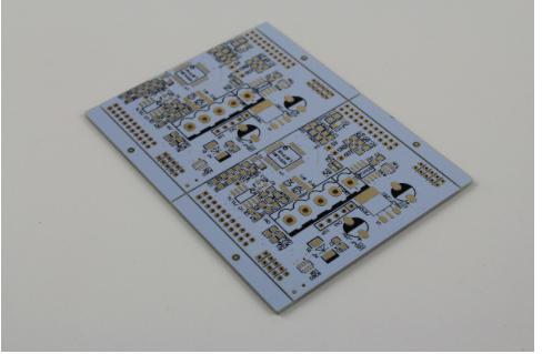
Rule 5: Repeat the required PCB circuit board on another larger circuit board to carry out the PCB board sampling and assembly. The equipment specifications applied by the right manufacturer can help reduce prototyping and manufacturing costs. First, carry out the layout of the PCB circuit board on the panel, contact the board manufacturer to obtain the selected specifications of each panel, then adjust your design specifications, and try to repeat your design multiple times within these panel specifications.
Rule 6: Integrate module values. As a designer, you will choose a discrete module with a high or low module value but the same performance. By integrating within a smaller normal value range, BOM can be simplified and costs can be reduced. If you have a series of PCB board samples based on the selected equipment value, it will also be more conducive to you to make appropriate inventory management decisions in a longer period of time.