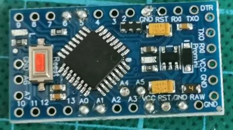
In the process of PCB design and production, the printed circuit board is what we usually call the PCB board, and its principle is the printed circuit board made in advance on the insulating base material.
According to the number of layers of the circuit board, we can simply divide the circuit board into single-sided, double-sided and multi-layer boards.
To put it simply, a single-sided board means that one side of the circuit board has a component surface, and the other side is wired and soldered; a double-sided board has wiring on both sides, and the two sides rely on vias for connection. The vias for this connection can be made according to requirements There are two types of PTH and NPTH. The difference between these two types of vias is whether there is sinking copper in the vias; multi-layer boards generally use PTH vias because they involve the lines of the middle interlayer.

When designing the PCB board, we also have a set of rules: first arrange the positions of the main components according to the signal flow, and then follow the "circuit is difficult first, then easy, the volume of the components is from large to small, strong signal and weak signal are separated, high and low Separate the signals, separate the analog and digital signals, try to make the wiring short and the layout of the PCB as reasonable as possible”. Pay special attention to the separation of the “signal ground” and the “power ground”; this is mainly to prevent power The ground wire sometimes has a large current passing, if this current is introduced into the signal end, it will be reflected to the output end through the chip, thereby affecting the voltage regulation performance of the switching power supply.
Then, the arrangement position and wiring direction of the components should be consistent with the wiring of the circuit diagram as much as possible, so that it will be much more convenient for later maintenance and testing.
The ground wire should be as short and wide as possible, and the printed wires that pass the AC current should be as wide as possible. Generally, we have a principle when wiring, the ground wire is the widest, the power wire is second, and the signal wire is the narrowest.
Minimize the feedback loop, input and output rectifier filter loop area as much as possible, this purpose is to reduce the noise interference of the switching power supply.
Inductive components such as thermistors should be as far away as possible from heat sources or circuit components that may cause interference.
The mutual distance between the dual in-line chips should be greater than 2mm, and the distance between the chip resistor and the chip capacitor should be greater than 0.7mm.
The input filter capacitor should be as close as possible to the line to be filtered.
In the PCB board design of PCB manufacturers, the most common problems are safety regulations, EMC and interference problems. In order to solve these problems, we should pay attention to the design: space distance, creepage distance and insulation penetration distance. The influence of three factors.
For example: Creepage distance: When the input voltage is 50V-250V, L-N in front of the fuse is ≥2.5mm, when the input voltage is 250V-500V, L-N in front of the fuse is ≥5.0mm; Clearance: When the input voltage is 50V-250V, Before the fuse, L-N≥1.7mm, when the input voltage is 250V-500V, before the fuse, L-N≥3.0mm; after the fuse, there is no requirement, but try to keep a certain distance to avoid short circuit damage to the power supply; primary side AC to DC part ≥2.0 mm; primary side DC ground to ground ≥4.0mm, such as primary side ground to earth; primary side to secondary side ≥6.4mm, such as optocoupler, Y capacitor and other component parts with foot spacing ≤6.4mm, slotting is required; two-stage transformer Between ≥6.4mm or more, ≥8mm reinforced insulation.