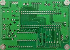
Depending on the decision to use or not to use a multilayer PCB, the process of creating a PCB may have similar results. Many PCB designers use multilayer boards when not necessary. Doing so will complicate the design, increase manufacturing costs, and make on-site repairs or modifications almost impossible.
1. From the perspective of PCB design, it is very tempting to use multiple layers when designing a PCB. After all, the concept of "small but good" seems to be ubiquitous in electronic design. However, unless doing so is a major design consideration, there are many reasons to avoid small pitfalls. E.g:
Design complexity: When designing a multilayer PCB, all through holes and vias must be arranged correctly. Errors can affect current and cause installation problems. In addition, using an odd number of layers or different thicknesses for the inner layer may cause bending or distortion of the board, making it impossible to install or degrade to a test-only state. Bad. For communication applications, where various signal types are routed across multiple layers, performance issues may arise due to crosstalk or mismatched impedance.
Increased manufacturing costs: Manufacturing multilayer PCBs is much more expensive than other circuit boards. More materials are needed, more time is needed, and technicians must be highly skilled. Simply going from two to four layers can increase manufacturing costs by 100%.

2. Difficult or impossible bench maintenance: Like any manufacturing or manufacturing process, small errors do occur. Especially for boards with odd or variable size layers. For single-layer (or double-layer) PCBs, these PCB layouts or designs can usually be easily repaired, and the circuit board can still be used. If the problem lies in the internal layers, this is practically impossible, and the board is useless.
Another problem that is sometimes overlooked is the increase in heat due to the added layers, which may not appear for a while until the product enters the site. If the product malfunctions seriously, this may lead to three Rs: recall, redesign and remanufacturing.
As we have seen, choosing a multilayer PCB can cause serious problems if it is not done properly. However, there is a bright side. If we are deliberate in the selection and design process, we can ride in the sun like Clint.
Multilayer power supply
3. Now, if you are willing to spend extra time on design and manufacturing, pay higher costs, and follow the best multi-layer PCB design guidelines, then you should continue with the multi-layer PCB option. Especially if size is the main concern. Let us assume it is not. What are the reasons for using multilayer PCBs?
Function: Multi-layer PCB allows the use of more complex circuits. Therefore, more functions can be built into a smaller package. This marketing advantage is very obvious. good.
Durability: Since attention and other considerations must be incorporated into multilayer PCB design and development, they are better constructed components and very reliable.
Installability: The smaller the PCB, the easier the installation. It requires fewer mounting holes and can be placed in more locations within a larger system. In fact, it can reduce the size of the entire product, which can increase portability, storage options and marketability.
Real design
4. The cost of multi-layer boards is higher, the production time is longer, and more professional knowledge is required to design and manufacture. Therefore, before deciding whether multiple layers are feasible, they should be carefully considered. When deciding whether to use a multilayer PCB, don't just focus on the "small" crowd. The result may be bad or very ugly. Instead, make choices based on reasonable decisions and weigh the pros and cons soberly to ensure good results.
No: Some PCB designs are more suitable for single-layer layout. A good example is the computer motherboard. These boards usually have many ports or various sizes, not to mention the need to be detachable. This will not make the use of multi-layer designs impossible; however, since the benefits of size reduction will not outweigh the disadvantages of increased complexity and cost, this is impractical.
5. Yes: The biggest reason for choosing a multi-level PCB design is to reduce the space occupied by the circuit board. In the case that design flexibility is not limited by the number of inputs and outputs, fan-out requirements of a single IC (ie MPU, FPGA, etc.) or similar trace length restrictions, multiple layers may be the way to go. This is especially true when the product allows the use of flexible circuits, which can eliminate most of the precision difficulties in the manufacturing process while giving more freedom.
Don't be content with using the same PCB for every design, be sure to choose the method that suits you best.
Single, double-layer or multi-layer PCB, the smooth and efficient software of AltiumDesigner® will enable you to use the PCB for the most effective and precise design.