How do we ensure the quality of our customers' PCB boards?
First of all, before production, we will purchase the correct materials according to the engineering materials or design materials, samples provided by the customer, and repeatedly confirm that our engineering and purchasing personnel have been in the PCB circuit board industry for more than 20 years, and can guarantee the accuracy of materials and projects. sex.
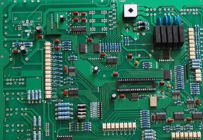
Secondly, we have a rigorous production process, and each step is traceable and standardized. Let's take a look at how we can ensure the quality of our customers' PCB boards in each production step. See the PCB process flow for details
Step
1. Substrate.
Use the data matrix to automatically check according to the order details. Material data (type, manufacturer, laminate and copper foil thickness) will be entered into the job history and displayed in the final Passport.
2. Print and etch the inner layer.
Visual inspection.
This step includes 3 visual inspections:

After printing and stripping, make sure that the unnecessary etching resist has been completely stripped
After etching, make sure that all unnecessary copper is etched away.
At the end of the process, make sure that all the resist has been stripped off the board.
Sampling inspection.
Each production panel has a specially developed test sample, which shows that the board has been etched correctly and the track width and isolation distance are correct. The type of etch resist used and the track width, isolation distance and annular ring values are all entered into the Passport file.
3. Check the inner copper pattern.
We use automatic optical inspection equipment to scan the inner copper layer and compare it with the design data. The machine checks whether all track widths and isolation distances correspond to the design values, and there is no short circuit or open circuit that will cause the finished board to malfunction.
4. Multi-layer bonding.
Material.
Use the data matrix to automatically check according to the order details. Material data (type, manufacturer, prepreg and copper foil) will be entered into the job history and displayed in the final Passport.
The thickness after bonding.
This is measured on each production panel, and the result is entered in Passport.
5. Drilling.
The drilling machine automatically checks the diameter of the drill bit to ensure that the hole size is correct. The special sample on the multilayer board confirms the position of the drilled hole relative to the (printed) inner layer.
The smallest finished hole size is input into Passport.
6. Hole wall preparation.
We deposit a layer of carbon on the wall of the hole to make it conductive for electroplating. We will enter Passport.
7. Apply electroplating layer
Visual inspection.
After printing and stripping, make sure that the unnecessary plating resist is cleanly stripped off
Enter Passport for the type of resistance.
8. Copper and tin plating.
Non-destructive sample inspection.
The operator measures the copper thickness in 5 or more holes on a panel on each flying pole. The result is entered in Passport.
9. Outer layer etching
Visual inspection.
After etching, make sure that all unnecessary copper is etched away.
Sampling inspection.
Each production panel has a specially developed test sample, which shows that the board has been etched correctly and the track width and isolation distance are correct. The type of etch resist used and the track width, isolation distance and annular ring values are all entered into the Passport file.
10. Solder mask.
in the process.
Visual inspection:
Each panel is evenly coated with solder mask (paint)
Soldering mask photoelectric tool and PCB alignment
Sample inspection:
The operator uses a projection microscope to inspect each panel to ensure that the solder mask is properly aligned and there are no solder mask traces on the pads.
Check the adhesion of the solder mask to the PCB surface through the tape test used after the legend is printed.
The type of solder mask used is entered in Passport data.
11. Surface treatment
Inspection of all surface treatment samples:
Use X-ray range to measure thickness.
We use the tape test after printing the legend to check the adhesion of the surface finish to the PCB surface.
100% visual inspection.
1. Lead-free hot air leveling.
The surface must be flat, even on the PCB, without any non-wetting conditions. The component holes must not be narrowed or blocked. If it is not covered by the solder mask, some through holes may be blocked.
2. Electroless gold plating on nickel.
The surface treatment must cover all exposed copper and have the same color on the PCB. There should be no discoloration even in the hole
3. Chemical silver.
must not be stained or blackened.
The surface treatment used enters Passport, even if the order is "Any leadfree".
For the surface treatment of gold and silver, we also enter the actual measured value.
12. Component legend.
Sample inspection after curing:
The operator conducts a tape test to check the surface finish, the adhesion of the solder mask and the legend to the PCB surface. We pressed a piece of pressure-sensitive tape on the test area and then pulled it out. There should be no copper, surface coating, solder mask or legend ink adhering to the tape.
Visual inspection.
The operator checks whether the legend on each board is clean and clear, and there is no blur or stain.
13. Electrical testing.
All circuit boards have undergone electrical testing, except for single-sided circuit boards that can be selected for electrical testing.
shorts and open circuit.
We build a netlist from Gerber and drill into the data. We use it as a reference netlist to test whether all networks have undergone short-circuit and open-circuit tests. The pass is recorded in the passport. As an extra precaution, if your design system outputs the IPC-D-356A netlist format, please include the file in your data set. Then we can use it to check the Gerber netlist on your design netlist.
14. Sectioning and milling.
We use special specimens to check the profile of the sheet and the size and position of the internal milling.
15. Final inspection.