For experienced engineers, PCB circuit design is very simple, all kinds of matters needing attention and operation skills are handy, very skilled. For new engineers, PCB circuit design skills are difficult, after all, their own proficiency is not good, there will be problems in design. Therefore, it is necessary to understand the circuit design of line PCB. So, what are the PCB circuit design skills?
What are the precautions and operation skills of PCB circuit design of ipcb company

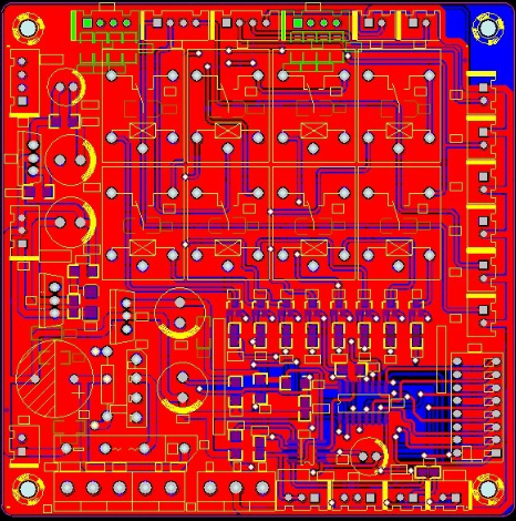
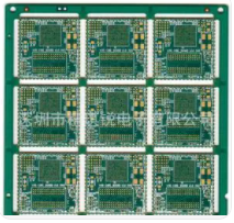
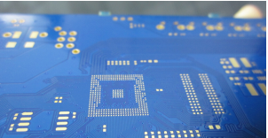
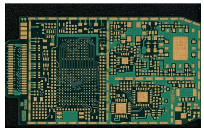
PCB circuit design
Tip 1: the definition of processing level should be clear
When the document is not clear, we must check with the engineer, so as to reduce the probability of plate making error. In addition, when designing a single-sided PCB circuit, special instructions should be paid attention to. If there is no special description, such as positive and negative, the PCB designed may not be soldered, so attention should be paid.
Tip 2: the distance between the copper foil and the outer frame should not be too close
According to the engineer's experience, the distance between the large area copper foil and the outer frame should be less than 0.2mm. Therefore, special attention should be paid to the operation. If the distance is less than 0.2mm, the solder resist may fall off.
Tip 3: do not draw pads with filler blocks
This technique is ignored by many novices, because it is possible to draw pads with filler blocks in PCB circuit design, which can pass the DRC inspection, but can not be used in processing, because such pads cannot directly generate solder mask. When solder resist is applied, the area will be covered by solder resist, which makes it very difficult to weld components.
Tip 4: electric layer can not spend pad and wire coexist
According to the editor's understanding, some engineers in PCB circuit design, the electrical layer will appear again is the flower pad, is the connection situation, this kind of situation is not right. Because the stratum is not the same as the actual printed on-board image, they are the opposite. All the wires are barrier wires and can not leave gaps, otherwise it is easy to cause power short circuit.
Tip 5: pads should not be too short
If the pad of surface mounted components is too short, it is easy to have the wrong test pin. Because there are too dense pads, the space between the two feet is very small, and the pads are very thin. When installing the test pin, it must be staggered up and down, otherwise this situation will occur.
Tip 6: pads cannot overlap
The overlap of pads can easily lead to scrapping during drilling. Therefore, the pads must not overlap.
The above are the six skills of PCB circuit design, which belong to skilled skills. These skills will not be too high, but they will greatly affect the results of PCB circuit design. Therefore, in the PCB circuit design process, we must pay attention to these points, so as to achieve perfection.