


In the process of PCB board design and production, engineers not only need to prevent PCB board from accidents in manufacturing process, but also need to avoid design errors.
ipcb summarizes and analyzes several common PCB problems, hoping to bring some help to everyone's design and production work.
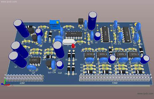
PCB board design
Problem 1: PCB board short circuit
This problem is one of the common faults that can directly cause the PCB to fail to work, and there are many reasons for this problem. We will analyze them one by one.
The reason of PCB short circuit is that the pad is not designed properly. At this time, the round pad can be changed into ellipse to increase the distance between points to prevent short circuit.
Improper design of PCB parts direction will also cause board short circuit and fail to work. For example, if the foot of SOIC is parallel to the tin wave, it is easy to cause a short circuit accident. At this time, the direction of parts can be appropriately modified to make it perpendicular to the tin wave.
There is also a possibility of PCB short circuit fault, that is, the automatic plug-in bending. Because the length of the wire pin is less than 2mm and the parts will fall off when the angle of the bending foot is too large, it is easy to cause short circuit. Therefore, the solder joint should be more than 2mm away from the line.
In addition to the three reasons mentioned above, there are also some reasons that can lead to PCB short-circuit fault, such as too large base plate hole, too low temperature of tin furnace, poor solderability of board surface, solder mask failure, board surface pollution, etc., which are relatively common fault causes. Engineers can eliminate and check the above reasons and fault conditions one by one.
Problem 2: dark and granular contacts appear on PCB board
The problem of dark or small granular joints on PCB board is mostly due to the contamination of solder and the excessive oxide mixed in the dissolved tin, resulting in the formation of solder joint structure which is too brittle. Attention should be paid not to be confused with the dark color caused by the use of low tin content solder.
Another reason for this problem is that the composition of solder used in the process of processing and manufacturing changes, and the content of impurities is too much, so pure tin should be added or replaced. The physical change of glass fiber layer, such as separation between layers. But this is not a bad solder joint. The reason is that the substrate is too heated, so it is necessary to reduce the preheating and soldering temperature or increase the travel speed of the substrate.
Problem 3: PCB solder joint turns golden yellow
Generally, the solder of PCB is silver gray, but occasionally there are golden solder spots. The main reason for this problem is that the temperature is too high, so we only need to lower the temperature of tin furnace.
Problem 4: the bad board is also affected by the environment
Due to the structure of PCB itself, it is easy to cause damage to PCB when it is in an unfavorable environment. Extreme temperature or temperature variation, excessive humidity, high-intensity vibration and other conditions are the factors leading to the performance degradation or even scrapping of the board. For example, changes in ambient temperature can cause deformation of the board. Therefore, the solder joint will be damaged, the shape of the board will be bent, or the copper trace on the board may be broken.
On the other hand, moisture in the air can cause metal surface oxidation, corrosion and rust, such as exposed copper traces, solder joints, pads and component leads. The accumulation of dirt, dust or debris on the surface of components and circuit boards can also reduce the air flow and cooling of components, resulting in overheating and performance degradation of PCB. Vibration, dropping, striking or bending PCB will deform and cause cracks, while high current or over-voltage will lead to PCB breakdown or rapid aging of components and channels.

Problem 5: PCB open circuit
An open circuit occurs when the trace breaks, or when the solder is only on the pad and not on the component lead. In this case, there is no adhesion or connection between the component and the PCB. Like short circuits, these can also occur during production or welding and other operations. Vibration or stretching of circuit boards, dropping them, or other mechanical deformation factors can destroy traces or solder joints. Similarly, chemical or moisture can cause solder or metal parts to wear, resulting in component lead breakage.
Problem 6: looseness or dislocation of components
During reflow soldering, the small parts may float on the molten solder and eventually leave the target solder joint. The possible reasons for the shift or tilt include the vibration or bounce of the components on the PCB due to insufficient support of the circuit board, setting of the reflow furnace, solder paste problems, human errors, etc.
Question 7: Welding
The following are some problems caused by poor welding practices:
Disturbed solder joint: solder moves before solidification due to external disturbance. This is similar to the cold solder joint, but the reason is different. It can be corrected by reheating, and the solder joint can be free from external interference when it is cooled.
Cold welding: this occurs when the solder cannot be melted properly, resulting in rough surfaces and unreliable connections. Since excessive solder prevents complete melting, cold solder joints may also occur. The remedy is to reheat the joint and remove excess solder.
Solder bridge: this happens when the solders cross and physically connect the two leads together. These may form unexpected connections and short circuits, which may cause the components to burn or the wiring to burn out when the current is too high.
Pad: insufficient wetting of pins or leads. Too much or too little solder. Pads raised due to overheating or rough welding.
Question 8: human error
Most of the defects in PCB manufacturing are caused by human error. In most cases, the wrong production process, the wrong placement of components and the lack of manufacturing specifications lead to 64% of the avoidable product defects. The potential for defects increases with the complexity of the circuit and the number of production processes due to the following: densely packed components; multiple circuit layers; fine wiring; surface soldered components; power and ground.
Although every manufacturer or assembler hopes to produce PCB board without defects, there are several problems in the design and production process that cause continuous PCB problems.
Typical problems and results include the following: poor welding will lead to short circuit, open circuit, cold solder joint, etc.; dislocation of the board will lead to poor contact and poor overall performance; poor insulation of copper trace will lead to arc between traces; too close between copper trace and path will easily lead to short circuit risk; insufficient thickness of circuit board will lead to bending and breaking Crack.


