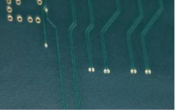
Step one of PCB design: Preliminary work of PCB copy board copy board
1. Use the schematic design tool to draw the schematic and generate the corresponding network table. Of course, in some special cases, such as the circuit board is relatively simple, there is already a network table, etc., it is not necessary to design the schematic diagram, and directly enter the PCB design system. In the PCB design system, you can directly use the parts and packaging. Generate a netlist.
2. Manually change the network table. Define the pads that are not on the schematic diagram such as the fixed pins of some components to the network connected to it. If there is no physical connection, it can be defined to the ground or the protective ground. Change the pin names of some devices with inconsistent pin names in the schematic diagram and PCB package library to be consistent with those in the PCB package library, especially diodes and transistors.
The second step of PCB design: draw the package library of non-standard devices defined by yourself
It is recommended to put all the parts drawn by yourself into a special design file for PCB library created by yourself.

The third step of PCB design: Set up the PCB design environment and draw the printed circuit board frame with hollow in the middle, etc.
1. The first step after entering the PCB copy system is to set up the PCB design environment, including setting the grid size and type, cursor type, layout parameters, wiring parameters and so on. Most of the parameters can use the system default values, and after these parameters are set, they are in line with personal habits and do not need to be modified in the future.
2. Planning the printed circuit board is mainly to determine the frame of the circuit board, including the size of the circuit board and so on. Put a proper size pad on the place where the fixing hole needs to be placed. For 3mm screws, 6.5~8mm outer diameter and 3.2~3.5mm inner diameter pads can be used. For standard boards, they can be imported from other boards or PCB izards.
Note: Before drawing the border of the circuit board, the current layer must be set to the Keep Out layer, that is, the wiring layer is prohibited.
The fourth step of PCB design: After opening all the PCB copy library files to be used, import the netlist file and modify the part package
This step is a very important part. The netlist is the soul of PCB automatic routing, and it is also the interface between the schematic design and the impression circuit board design. Only after the netlist is loaded, can the circuit board be wired.
In the process of schematic design, ERC inspection will not involve the packaging of parts. Therefore, when designing the schematic diagram, the packaging of the parts may be forgotten. When the netlist is introduced, the packaging of the parts can be modified or supplemented according to the design situation.
Of course, you can manually generate the netlist directly in the PCB, and specify the part package.
Step 5 of PCB design: lay out the position of the circuit board copy board parts package, also known as the part layout