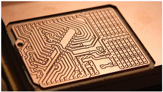
Resistance and capacitance factors in PCB design
1. Conductor resistance
Normally the current carrying capacity of the wire is not a problem; But ohmic resistance can be a problem when the wires are long and the voltage regulation requirements are strict. The resistance and temperature can also be calculated by the following formula:

R = 0.000227w
Where R is the resistance value per inch of wire length, measured in ohm; W is the width of the wire, in inches; It is based on a minimum copper purity of 99.5 percent and a thickness of 0.0027 inches (2 ounces).
2. Conductor capacitance
Capacitance may be quite important, especially in the high frequency range. When high-frequency circuits are involved, the distributed capacitance of one wire between the wires above another wire must be considered; It's about 1 picofart per foot. As a guide for approximation. The basic capacitance formula can be used:
Formula 1
When the conductor width is at least 10 times of dielectric distance, the calculated value is generally consistent with the actual measured value, but the calculated value may be a little lower. The coupling capacitance between the wires can be minimized by limiting the length of the wires in the same horizontal plane. The capacitance between adjacent wires is a function of the wire width, thickness, spacing and the characteristics of the plate itself, which can be calculated as follows:
Formula 2
Where, K = the dielectric constant of the base; A = Conductor thickness (in.); B = width of wire (in.); D = Distance between wires in inches
Special attention must be paid to circuits located on the shielded or ground plane, because the entire length of the conductor combined with the shielded or ground plane forms a capacitance, and the combination of similar conductors in the same case must also form a capacitance.
It has been pointed out that, for critical high circuits, the electrical characteristics of a one-side printed circuit made of 1/16 inch epoxy-glass or epoxy paper are not sufficient and must be a microstrip wire structure connected to the ground. Electrical characteristics can also be used as a means of process control and can clearly indicate the number of process parameters