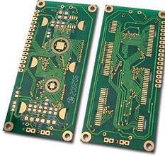
Circuit board solder mask introduction:
The solder mask bridge, also known as the green oil bridge and the solder mask dam, is a "isolation band" made by the factory to prevent short-circuit of the pins of SMD components. Solder mask opening is a measure taken for some special needs, such as heat dissipation of the positive board, good contact with the shell, and so on.
Green oil bridge is the green oil between SMD and SMD components (the width of the solder mask is reserved between the two solder mask windows, generally> 6mil), mainly to prevent short circuit. The following picture shows the PCB board with and without the green oil bridge.

The reason for the PCB board solder resist bridge falling off:
1. When the PCB is printed with ink, the pre-treatment is not in place, such as stains, dust or impurities on the surface of the PCB, or some areas are oxidized, but in fact, the simplest solution to this problem is to do the pre-treatment again. That's it, but try to clean the dirt, impurities or oxide layer on the surface of the PCB board. This is caused by the error of the production staff in the operation, and it is not strictly prohibited in the management.
2. It may be because it is out of the oven, the baking time of the PCB board is short or the temperature is not enough, because the PCB board must be baked at a high temperature after printing the thermosetting ink, and if the baking temperature or time is insufficient, it will As a result, the ink on the board surface is not strong enough. After the subsequent process flows, the final product is shipped. The customer receives the board for patch processing. The high temperature of the tin furnace during patch processing causes the PCB board ink to fall off.
3. Ink quality problems or ink expired, due to the greed for cheap when purchasing, the purchase of the same brand of ink and the price difference of the problem ink, or the purchase of small ink from an unknown brand, this will also cause the PCB board ink to be too tinted. The furnace is falling. In some small board factories, the purchased ink has not been used up for a long time, and the color is different after repeated use, the performance is also greatly reduced, and the ink is more likely to fall off.
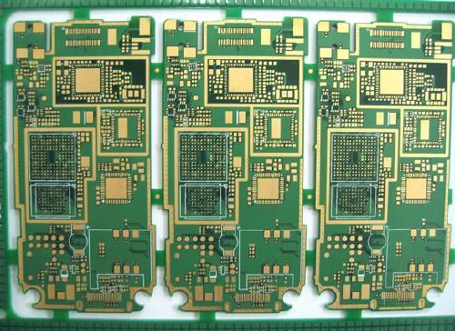
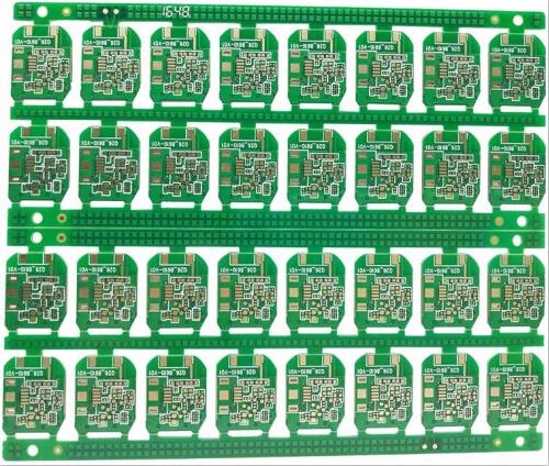
PCB board copper foil thickness
The thickness of the copper foil refers to the thickness formed by the copper foil covering the board.

The thickness of the copper skin of the PCB board national standard is mainly 35um; 50um; 70um.
For PCB boards with a copper thickness of 150um, the manufacturers basically use plating. This process is difficult, and the general manufacturers are unwilling to produce and the cost is extremely expensive, which is not suitable for mass production.
Suggestion: For the wiring of the module with extra large power supply, if the entire board does not require 150um, you can consider adding tin manually or adding a high-current copper conductor in parallel. This process is convenient for operation and can be mass-produced.
Circuit board thickness
The thickness of the printed circuit board (PCB) refers to the thickness after the board is completed. It should be determined according to the function of the printed circuit board, the weight of the installed device, the overall size and the mechanical load it bears, and the specifications of the printed socket.
The nominal thickness of copper clad laminates is 0.5, 0.7, 0.8, 1.0, 1.2, 1.5, 1.6, 2.0, 2.4, 3.2, 6.4 mm. Paper-based copper-clad laminates with nominal thicknesses of 0.7 and 1.5 mm and glass cloth-based copper-clad laminates with nominal thicknesses of 0.5 and 1.5 mm are suitable for printed plugs. The thickness tolerance of the printed plug area is very important, it will affect the reliable contact with the socket, so it must be matched with the selected socket.
1.5 mm thick printed circuit boards are widely used in various electronic instruments and equipment. Because the thickness of the printed board is enough to support the weight of integrated circuits, medium and low power transistors and general resistance-capacitance components. Even if the printed board area is as large as 500*500 mm, there is no problem. A large number of sockets are used in conjunction with printed boards of this thickness.
The thickness of the printed circuit board for power supply is thicker, because it needs to support heavier transformers, high-power devices, etc., generally 2.0 to 3.0 mm thick can be used. As for some small electronic products, such as electronic watches, calculators, etc., there is no need to choose such a thick sheet, 0.5 mm or thinner is sufficient.
The thickness of a multilayer printed board is related to its number of layers, and the thickness of a multilayer board with 8 layers or less can be limited to about 1.5 mm. The thickness of more than 8 layers should exceed 1.5 mm. The thickness between each circuit layer of a multilayer board is often determined by electrical design.