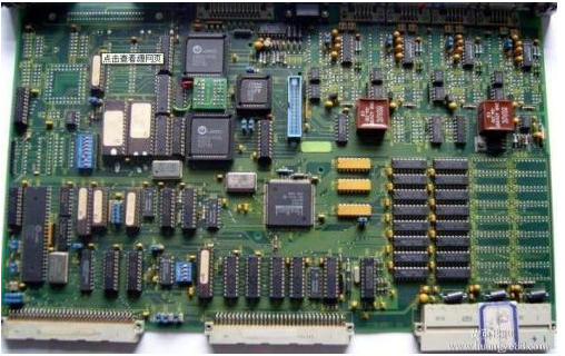
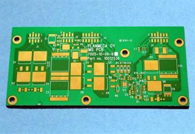
Plating film produced during multi-layer PCB proofing process
With the rapid development of the PCB industry, PCB is gradually moving towards the direction of high-precision thin lines, small apertures, and high aspect ratios (6:1-10:1). The hole copper requirements are 20-25Um, and the DF line spacing is less than 4MIl. Generally, PCB companies have problems with electroplating interlayers. The following editor will talk about the causes of electroplating interlayer film in the multi-layer PCB proofing process and how to improve the treatment.
The following is an explanation of the reasons for the electroplating interlayer during the multi-layer PCB proofing process.
1. The pattern of the board is not uniformly distributed. During the pattern electroplating process, due to the high potential of several isolated lines, the plating layer exceeds the film thickness, forming a sandwich film and causing a short circuit.
2. The anti-plating film layer is too thin. During electroplating, the plating layer exceeds the film thickness, forming a PCB sandwich film. In particular, the smaller the line spacing, the easier it is to cause the film short circuit.

Two reasons for electroplating interlayer in the process of multi-layer PCB proofing and how to improve the treatment
Method for improving electroplating interlayer film in multi-layer PCB proofing process
1. Increase the thickness of the anti-plating layer: choose a dry film with a suitable thickness. If it is a wet film, you can use a low-mesh screen printing, or increase the film thickness by printing the wet film twice.
2. The board pattern is not evenly distributed, and the current density (1.0~1.5A) can be appropriately reduced for electroplating. In daily production, we want to ensure the output, so we usually control the electroplating time as short as possible, so the current density used is generally between 1.7 and 2.4A.
In this way, the current density obtained in the isolated area will be 1.5 to 3.0 times that of the normal area, which often results in the coating height of the isolated area with a small distance exceeding the film thickness by a lot. The phenomenon that the edge clamps the anti-coating film, which causes the film short circuit, and at the same time makes the thickness of the solder mask on the circuit thinner.
iPCB is a high-tech manufacturing enterprise focusing on the development and production of high-precision PCBs. iPCB is happy to be your business partner. Our business goal is to become the most professional prototyping PCB manufacturer in the world. Mainly focus on microwave high frequency PCB, high frequency mixed pressure, ultra-high multi-layer IC testing, from 1+ to 6+ HDI, Anylayer HDI, IC Substrate, IC test board, rigid flexible PCB, ordinary multi-layer FR4 PCB, etc. Products are widely used in industry 4.0, communications, industrial control, digital, power, computers, automobiles, medical, aerospace, instrumentation, Internet of Things and other fields.