Difficulties in the production of multi-layer circuit board proofing1
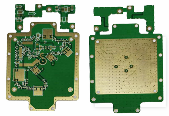
What are the production difficulties of multi-layer circuit board proofing! In the circuit board industry, multi-layer circuit boards (high-precision PCB multi-layer boards) are generally defined as 4 layers-20 layers or more called multi-layer circuit boards, which are better than traditional multi-layer circuit boards. Circuit boards are difficult to process and require high quality and reliability. They are mainly used in communication equipment, industrial control, security, high-end servers, medical electronics, aviation, military and other fields. In recent years, the market demand for high-level PCB boards in applications such as communications, base stations, aviation, and military has remained strong. With the rapid development of China's telecommunications equipment market, the market prospects for high-level PCB boards have been promising.
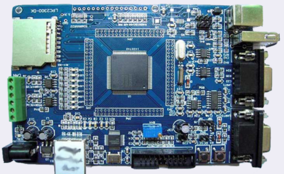
At present, domestic high-level circuit board manufacturers capable of circuit board proofing production mainly come from foreign-funded enterprises or a few domestic-funded enterprises. The production of high-level circuit boards not only requires high technology and equipment investment, but also requires the accumulation of experience of technicians and production personnel. At the same time, the import of PCB multilayer circuit boards has strict and cumbersome customer certification procedures. Therefore, the barriers for multi-layer circuit board proofing to enter the enterprise are relatively high. High, the realization of industrialized production cycle is longer. The PCB proofing products of Shenzhen Technology Co., Ltd. are positioned on the 1-30 layer, mainly for high-precision double-sided/multi-layer proofing production.

The average number of layers of PCB multi-layer boards has become an important technical indicator to measure the technical level and product structure of PCB companies. This article briefly describes the main processing difficulties encountered in the production of multi-layer circuit board proofing, and introduces the control points of the key production process of high-level circuit boards for your reference.
1. Difficulties in making main circuit boards
Compared with the characteristics of conventional circuit boards, high-level circuit boards have the characteristics of thicker PCB boards, more layers, denser lines and vias, larger unit sizes, thinner dielectric layers, etc., inner layer space and interlayer alignment., Impedance control and reliability requirements are more stringent.
1. Difficulties in alignment between layers
Due to the large number of high-level PCB layers, the customer design side has more and more stringent requirements for the alignment of each layer of the PCB. Usually, the alignment tolerance between layers is controlled at ±75μm. Considering the high-level board unit size design and the ambient temperature and humidity of the graphics transfer workshop, And factors such as misalignment and superposition caused by inconsistency of expansion and contraction of different core layers, interlayer positioning methods, etc., make it more difficult to control the alignment of high-rise boards.
2. Difficulties in the production of the inner line
PCB high-level circuit boards use special materials such as high TG, high speed, high frequency, thick copper, thin dielectric layer, etc., which puts forward high requirements for the production of inner circuit and pattern size control, such as the integrity of impedance signal transmission, which increases the production of inner circuit Difficulty. Small line width and line spacing, more open and short circuits, more short circuits, and low pass rate; more fine line signal layers, the probability of missing AOI detection in the inner layer is increased; the inner core plate is thinner, which is easy to wrinkle and cause poor exposure and etching It is easy to roll the board when passing the machine. Most of the multi-layer circuit boards are system boards, and the unit size is relatively large. The cost of scrapping the finished product is relatively high.